Yield Improvement Changes the Question
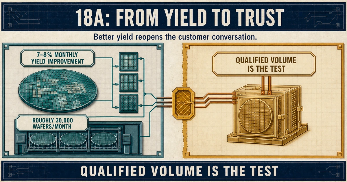
The 18A story has moved from “can the process work?” to a more uncomfortable question: can better yields become external customer commitments? The manufacturing signals have improved — the reported variability fix, the ~30,000-wafer trajectory, monthly yield gains in Tan’s own framing, and Tom’s Hardware reporting that yields are expected to reach Intel’s cost targets by end-2026 and industry-standard levels in 2027.
A BlueFin Research note reported by TechPowerUp said Intel had resolved wafer-to-wafer yield variability, with output across Fab 52 and Hillsboro moving toward roughly 30,000 wafers per month. TrendForce separately reported CEO Lip-Bu Tan’s description of monthly yield gains of 7-8% and expectations for customer commitments in the second half of 2026. These signals matter, but they remain reporting and company framing rather than a complete public disclosure of functional and parametric yield.
The commercial scoreboard tells the other half:
Q1 2026 foundry revenue (mostly internal)
external foundry revenue
foundry operating loss
The safer reading is not “Intel fixed everything.” It is that Intel may have improved 18A enough to reopen the customer conversation. The problem removed is a reported source of wafer-level inconsistency. The bottleneck created is harder to summarize in one number: Intel must now turn process stability into product-specific qualification, predictable delivery, acceptable cost, and signed external volume.
The Bottleneck Moves From Wafers to Qualification
Yield is not one number. Functional yield counts dies that operate at all. Parametric yield asks whether they meet performance, voltage, and power targets. Blended figures can hide differences among products, die sizes, configurations, and maturity levels. A process that works for Intel’s Panther Lake parts may still be unattractive for a large external AI accelerator. Bigger dies are generally harder to yield, and an outside design introduces its own libraries, IP, packaging, and validation requirements.
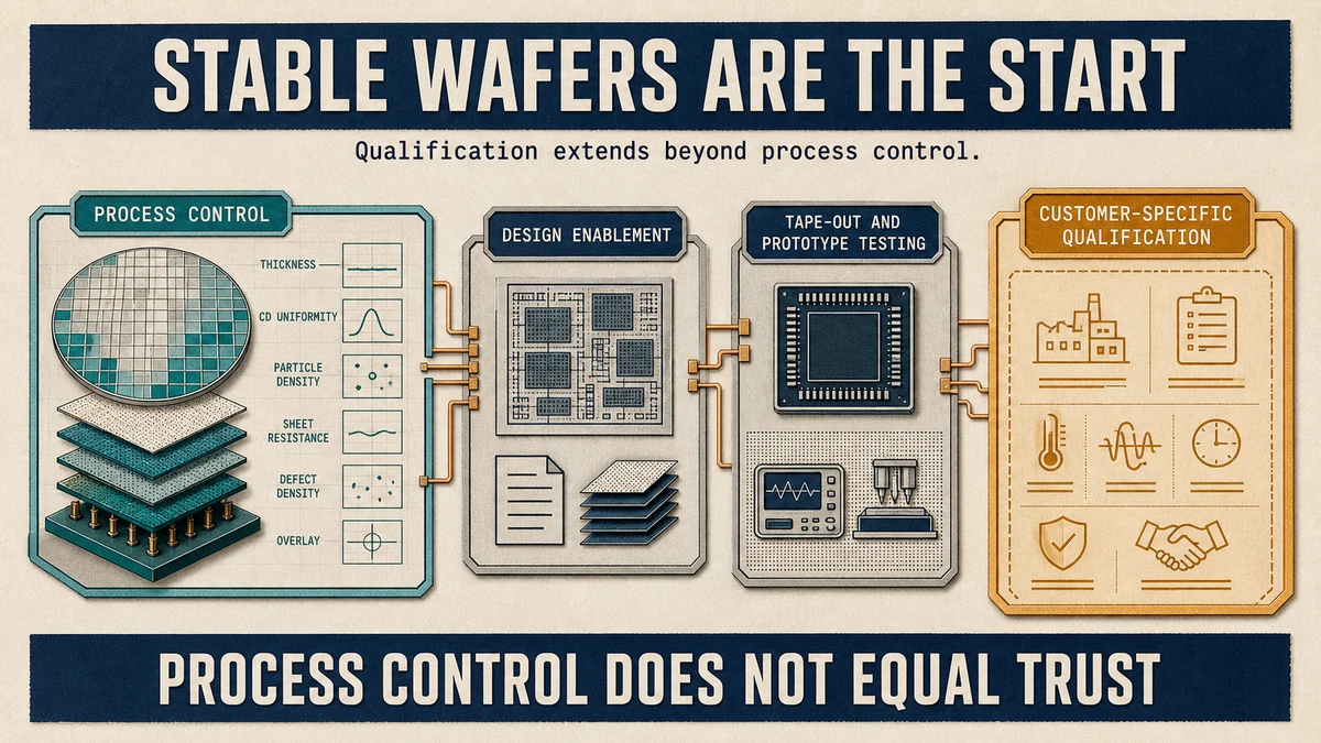
Resolving wafer-to-wafer variability would improve process control and make output more predictable. That can reduce uncertainty, sharpen learning cycles, and help cost planning. It does not prove that a customer’s exact design will repeatedly satisfy electrical, thermal, reliability, packaging, and schedule requirements. Customers do not need a perfect public yield number. They need enough private evidence to risk a tape-out.
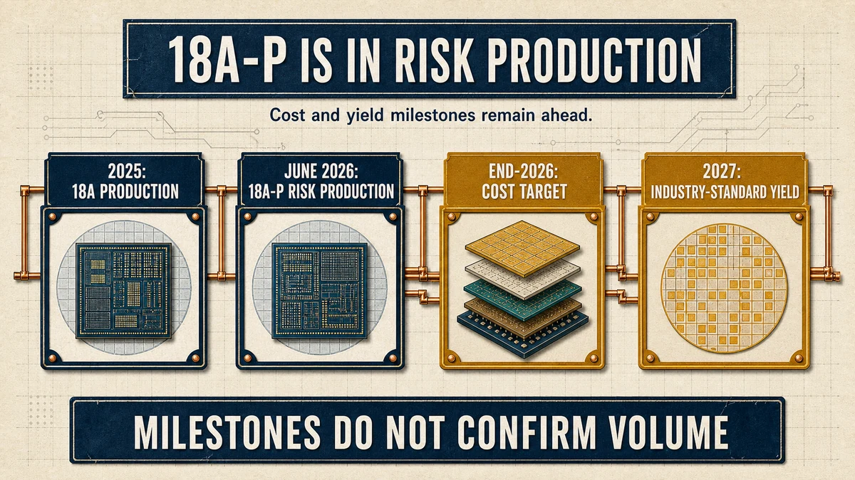
Intel’s June 2026 VLSI announcement adds useful but bounded evidence. The company said 18A entered production in 2025 and that 18A-P, its first performance enhancement in the family, had entered risk production. Intel also claimed that 18A-P delivers 9% higher performance at the same power or 18% lower power at the same performance than 18A. It cited improved thermal resistance, lower via resistance, additional transistor options, and design-rule compatibility with 18A.
Those statements describe Intel’s process progress. They do not identify an external product that has completed qualification or entered volume shipment. Risk production is a milestone on the way to a ramp, not the end of the commercial test.
Intel’s RAMP-C announcement points to progress in another part of the bottleneck. Intel said the program developed technology, IP, and design tools; onboarded early commercial and defense customers; and supported tape-out and testing of early prototypes. That is company-reported evidence of design enablement and prototype readiness. It does not establish recurring external volume, but it shows that qualification depends on more than the wafer process alone.
Captive Volume Does Not Prove Customer Trust
- Intel’s own products on 18A (Panther Lake and successors)
- Fills fabs, speeds learning cycles, debugs the node in-house
- Proves Intel can USE the process
- An outside company designs around Intel’s process and ecosystem
- Multi-year commitment: PDKs, design rules, capacity, packaging, schedules
- Proves customers TRUST Intel Foundry as a service
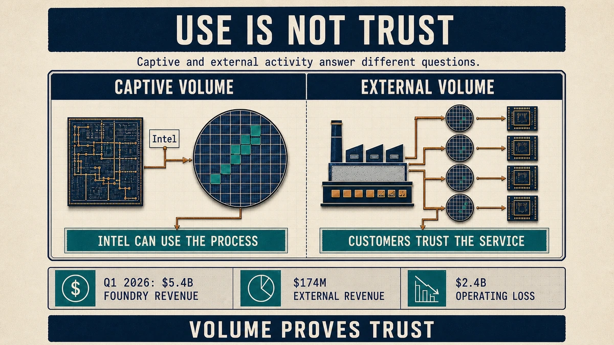
Captive demand gives Intel wafers to run, faster learning cycles, and a way to debug the node inside a product organization it controls. External demand asks another company to organize a product around Intel’s process design kit, design rules, IP ecosystem, packaging path, capacity plan, and delivery promises. One proves that Intel can use the process. The other proves that customers trust Intel Foundry as a service.
Microsoft is the strongest named external reference. It was publicly announced as an 18A customer at Foundry Direct Connect in February 2024. Later reporting points to a possible Maia AI accelerator on 18A or 18A-P, but that product pairing remains reported rather than confirmed by both companies. Precision matters: “announced customer” is firm; “Maia is definitely on 18A” is not.
Nvidia is the cleanest counter-example. Reporting described its $5 billion Intel stake as accompanied by product collaboration but not by a manufacturing commitment. The investment and foundry decision are separate signals. Nvidia may create value for Intel through collaboration without accepting Intel’s process risk for critical silicon. The useful question is not whether Nvidia helped Intel. It is whether Nvidia moved a product onto Intel’s process. On the supplied reporting, the answer remains no.
This distinction explains why Intel’s revenue mix matters. The Q1 2026 figures show $5.4 billion of foundry revenue but only $174 million of external foundry revenue, alongside a $2.4 billion operating loss. The numbers do not show that 18A cannot win customers. They show that Intel Foundry was still overwhelmingly supported by internal activity and that external scale had not yet settled the commercial argument.
| Measure | Reported | Basis |
|---|---|---|
| Foundry revenue, Q1 2026 | $5.4B | Mostly internal |
| External foundry revenue, Q1 2026 | $174M | Q1 2026 transcript |
| External share of foundry revenue | 3.2% | Computed from the two figures above |
| Foundry operating loss, Q1 2026 | $2.4B | Q1 2026 transcript |
| Monthly yield gain | 7–8% | CEO Lip-Bu Tan, via TrendForce |
| Wafer trajectory | ~30,000 / month | BlueFin note, via TechPowerUp |
| 18A-P vs 18A | +9% performance at equal power, or 18% lower power at equal performance | Intel, VLSI June 2026 |
| Cost-target milestone | End of 2026 | Reported expectation |
| Industry-standard yield | 2027 | Reported expectation |
Where Cost, Equipment, and Materials Enter the Test
Better yield should improve economics because more usable dies can absorb the cost of each processed wafer. Less variability can also reduce scrap, rework, investigation, and schedule disruption. But the supplied reporting places Intel’s cost-target milestone at the end of 2026 and industry-standard yield levels in 2027. The reported fix therefore removes one source of instability; it does not erase the cost gap in a single step.
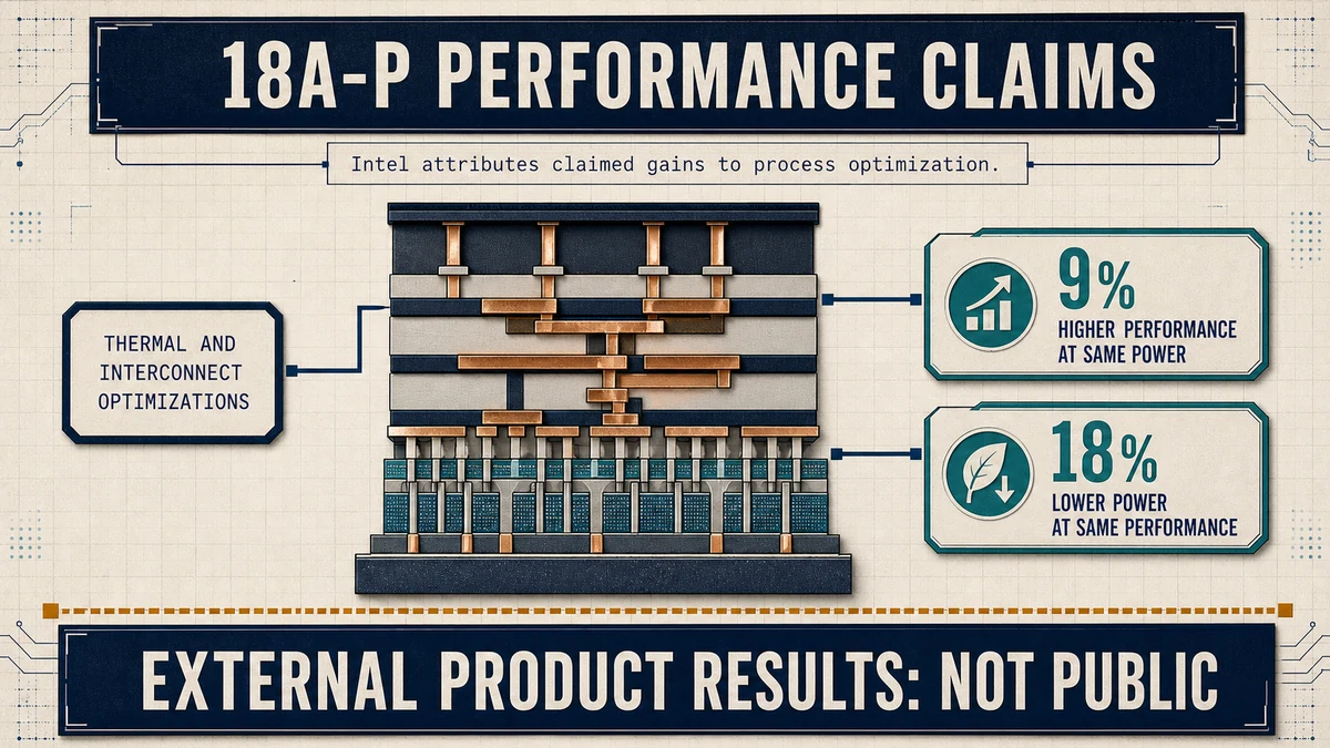
The equipment and materials effects are similarly layered. Intel attributes 18A-P improvements to transistor, interconnect, geometric, and materials optimization. Its VLSI update cites Power Boost, a dual-contact transistor option; improved thermal resistance; lower via resistance; PMOS strain engineering; and additional low-power and high-performance transistor choices. These are company claims, and they describe tools designers can use rather than disclosed external-product results.
More process capability can create value, especially if it improves performance per watt or makes heat easier to manage. It also creates qualification work. Models must reflect the options, IP must be validated against them, design flows must handle them, and production must demonstrate that the benefits persist across operating conditions and lots.
Intel says 18A-P is design-rule compatible with 18A, allowing more direct reuse of existing IP and design flows. If that works as intended, it can reduce migration friction, engineering cost, and qualification time. It cannot eliminate product-specific verification, reliability testing, packaging integration, or the need to protect the customer’s launch schedule.
Who Owns the Value and the Risk
Intel owns the upside from higher utilization, more usable dies, stronger process credibility, and a larger base of external revenue. It also owns the main manufacturing and service-execution risks: stable process control, enough usable capacity, dependable packaging, mature design enablement, and accurate communication when schedules or targets move.
External customers own a different concentration of risk. By tape-out, a customer has committed years of engineering, EDA flows, IP validation, and a product window. A foundry delay can cost more than wafer time because it can cause a product to miss the market it was designed to serve. Foundry trust is therefore an economic requirement, not a public-relations preference.
The risk does not disappear when the process improves. It moves. Intel first had to show that 18A could become a controllable manufacturing process. It must then prove that the broader system around the node can support outside designs. The customer must decide when Intel’s private evidence is strong enough to justify switching or adding a leading-edge supplier.
If that decision turns into qualified volume, Intel captures manufacturing revenue and strategic credibility while customers gain another advanced-node option. If schedules, yields, packaging, or design enablement disappoint, Intel absorbs underutilization and reputational damage while the customer absorbs redesign costs and a threatened market window. That distribution of risk is why a named design announcement matters less than a completed qualification and dependable ramp.
What Would Count as Conversion
The strongest next signal would be a named external 18A or 18A-P customer with product-level detail, a qualification or tape-out milestone, and committed capacity. Capacity is the tell in a foundry business because it shows movement beyond evaluation. A disclosed shipment milestone and external revenue attributable to the node would make the case stronger still.
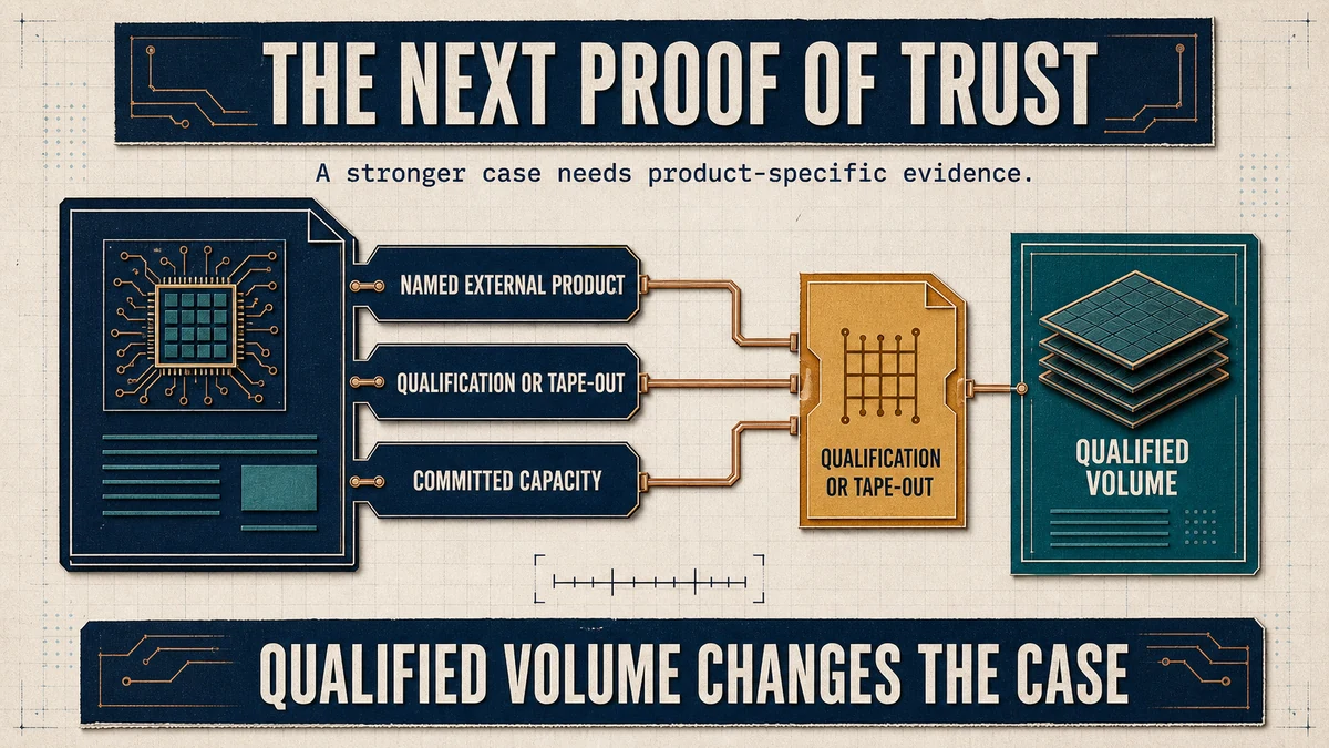
Other useful disclosures would include parametric yield rather than wafer volume alone, an official Intel-Microsoft product confirmation, and any Nvidia move from collaboration to manufacturing. No single disclosure would settle every issue. Together, they would show the bottleneck moving from process learning through qualification and into repeatable commercial production.
Is Microsoft an Intel 18A customer?
Microsoft was publicly named as an Intel 18A customer in February 2024, which makes it the strongest external reference. Later reports pairing specific Maia-generation AI chips with 18A remain reported claims until both companies confirm the product.
The 18A yield story is real enough to matter and not settled enough to overstate. Intel appears to have repaired the manufacturing conversation — necessary, maybe even the first condition of a credible foundry comeback, but not sufficient. Foundry is a trust business, and the second-half-2026 test is brutally simple: does better yield become signed external volume?
Later in this series
This article is for information and industry analysis only. It is not investment advice. Reported yield figures, customer discussions, and forecasts should be read as source-specific claims unless independently disclosed by the companies involved.
Sources
- TechPowerUp — BlueFin note: variability resolved, ~30,000 wafers/month (2026)
- TrendForce — 7–8% monthly yield gains; 2H26 customer expectations (2026-05-19)
- The Motley Fool — Q1 2026 transcript: $5.4B foundry / $174M external / −$2.4B (2026-04-23)
- The Washington Post — Nvidia $5B stake without a manufacturing commitment (2025-09-18)
View all sources
- Tom’s Hardware — cost-level end-2026, industry-standard 2027 (2025-10)
- Investopedia — Microsoft named at Foundry Direct Connect (2024-02)
- Wired — Microsoft/18A context (2024)
- Tom’s Hardware — reported Maia-on-18A claim (2026)
- PC Gamer — collaboration described as product-driven (2026)
- MarketWatch — Q1 foundry progress coverage (2026-04)
- Intel Foundry — 18A production status and company claims for 18A-P (2026-06-16)
- Intel Foundry — RAMP-C design enablement, prototypes, and early customer engagement (2026-07-28)