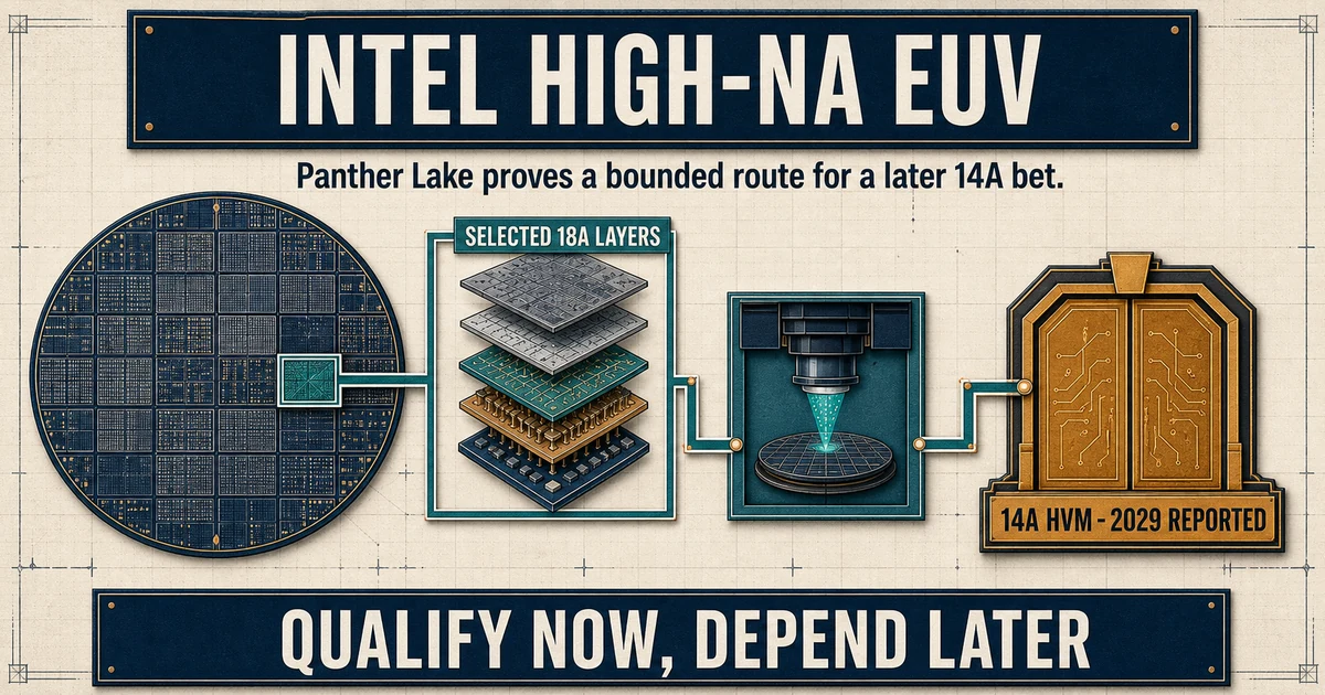
For a decade, Intel was the company that fell behind on lithography. Now it has shipped first – a high-volume logic chip built with the most advanced lithography tool ever sold – and the interesting part is that the chip barely needed it. That milestone came on July 15, 2026.
Panther Lake proves qualification, not dependency
ASML and Intel jointly confirmed that Intel Foundry is the first company to ship a high-volume logic product made with High-NA EUV. The chip is Panther Lake, Intel’s Core Ultra Series 3 processor. The production scanner is ASML’s TWINSCAN EXE:5200B, the second generation of its 0.55-NA platform and the successor to the EXE:5000 that Intel installed at its Oregon research site in 2024.
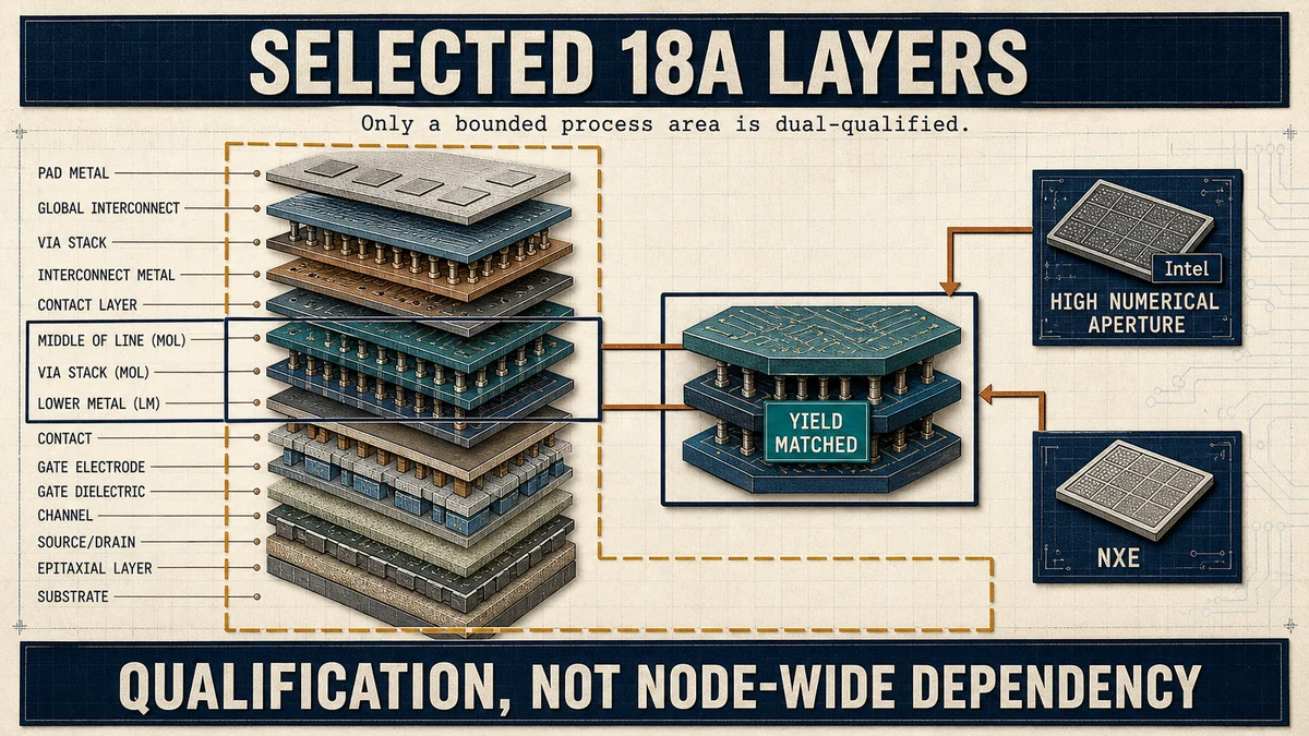
The important word in Intel’s account is not first. It is select. Only select Intel 18A layers are dual-qualified on High-NA and the established Low-NA NXE route. Intel also says the yields on those selected layers match its NXE tools. That is a useful manufacturing milestone, but it is a company claim about a bounded part of the process. It does not mean the whole node uses High-NA, and it does not mean 18A needed High-NA to become viable.
The supplied reporting cites a KeyBanc estimate that Intel 18A yield climbed from about 65% to roughly 85% over a quarter. That number is an analyst estimate, not an Intel disclosure. Even if it is directionally correct, it reinforces the distinction: 18A was already in commercial production on Low-NA equipment. A process at that stage does not need a scanner reported to cost about $380-400 million simply to finish Panther Lake.
So the immediate bottleneck was not basic 18A resolution or a last-minute Panther Lake yield rescue. It was qualification: proving that a High-NA route could coexist with an established NXE route on live wafers, match the incumbent yield on selected layers, and begin producing the operational evidence Intel will need later. Panther Lake is valuable because Intel controls the product and the manufacturing flow. It can introduce High-NA within a limited boundary, observe the consequences, and avoid making the entire node depend on an immature route.
14A is where the lithography economics change
The product that makes the early work strategically relevant is 14A. Intel’s own 2024 material described High-NA as a capability for process leadership beyond Intel 18A. Supplied roadmap reporting places the 14A PDK 0.9 design-rule lock around October 2026, risk production in the 2027-2028 window, and high-volume manufacturing in 2029. A broader external-customer variant, 14A-E, was placed in the 2028-2029 period.
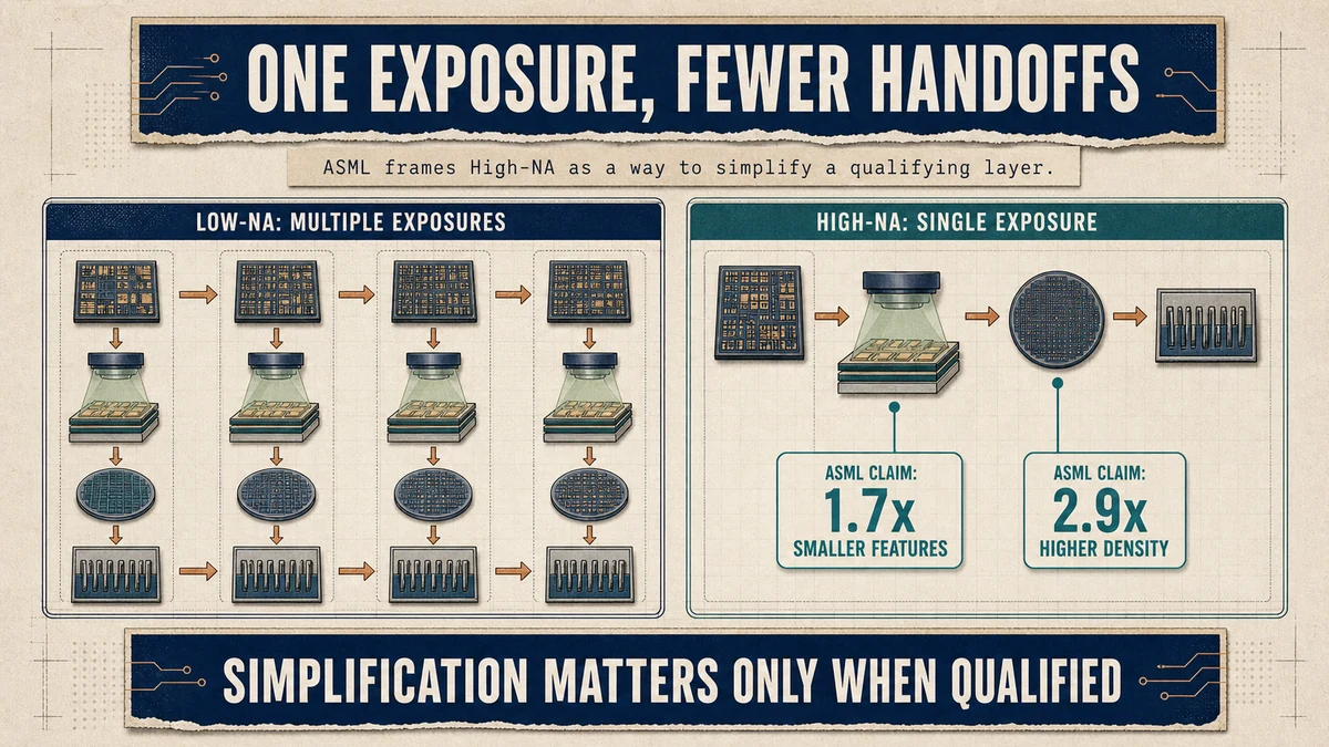
At the tightest pitches, the patterning problem changes. A conventional 0.33-NA EUV scanner may be unable to resolve a difficult layer in one exposure, forcing the fab to split the pattern across two or more exposures. Multi-patterning adds masks, alignment operations, etch steps, cycle time, and defect opportunities. The published baseline cites an industry rule of thumb that an additional pass can add on the order of 30% to that layer’s wafer cost. That is not a universal cost law, but it captures why another exposure is more than another trip through a scanner.
ASML says the EXE:5200B provides 8 nm resolution and 40% more imaging contrast than NXE systems. The company says it can print features 1.7 times smaller in a single exposure and support 2.9 times higher transistor density. These are ASML product claims, not independently demonstrated economics for Intel 14A. They nevertheless identify the problem High-NA is built to remove: the process complexity and cumulative error budget created when a single layer must be decomposed into several patterning operations.
Collapse two or three passes into one, and a qualifying layer can need fewer masks and etch operations. Cycle time can fall. There are fewer overlay relationships to control and fewer process steps at which defects can enter. Yield can benefit if the simpler route is stable. The qualification condition is crucial: a theoretically simpler sequence has no production value until it repeatedly meets the fab’s overlay, defect, uptime, and yield requirements.
This is why selected 18A layers matter. The exposures are not the main asset. The asset is accumulated operating evidence: uptime behavior, overlay drift, defect signatures, mask handling, maintenance routines, and the boundary conditions under which High-NA matches the NXE route. My read remains that Intel is trying to bank roughly two years of this learning before 14A customers need it. A competitor can buy the same model of scanner later. It cannot buy Intel’s earlier months of qualified wafer history.
The bottleneck moves to utilization and process control
High-NA does not eliminate the manufacturing bottleneck. It moves it.
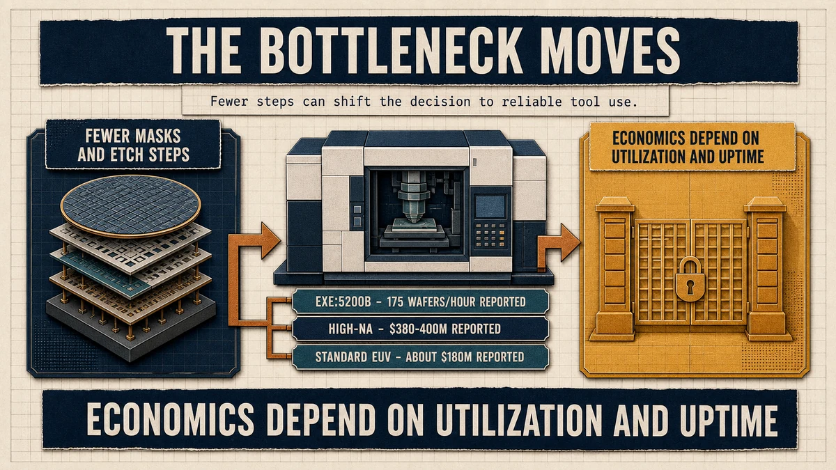
The problem removed is resolution-driven process multiplication. On a suitable layer, one higher-resolution exposure can replace multiple Low-NA exposures and some of the masks, alignments, and etch operations attached to them. The new bottleneck is making that single exposure economically dependable. A scanner reported at roughly $380-400 million costs more than twice the approximately $180 million cited for a standard EUV system. Reported EXE:5200B throughput is around 175 wafers per hour. Once the image can be printed, utilization, uptime, maintenance, overlay performance, and depreciation determine whether it should be printed that way.
The cost effect therefore runs in both directions. High-NA can reduce per-layer process complexity, work in progress, mask demand, and repeated patterning steps. It also concentrates more capital cost in one tool and raises the penalty when that tool is idle. A fab needs sufficient qualifying wafer volume to spread depreciation and sufficient reliability to keep the expensive capacity productive. Intel’s internal CPU volume gives it a structural way to feed the learning loop before external foundry demand is certain.
The yield effect is conditional as well. Removing exposures eliminates some alignment and defect opportunities, which can improve yield. But a new route introduces its own process-control work. Intel must show that matched yield on selected 18A layers becomes stable performance across the layers where 14A expects High-NA to carry more weight. The supplied evidence does not prove node-wide yield improvement from High-NA, and the approximately 85% 18A figure cannot be used for that purpose because it is an analyst estimate for the node rather than a disclosed comparison of lithography routes.
Qualification is the bridge between equipment capability and economic value. Intel must qualify masks, overlay controls, defect inspection, recipes, maintenance behavior, and integration with adjacent process steps. The available evidence supports fewer masks and etch operations when multi-patterning is removed. It does not separately establish a broad advantage in resist or other material consumption, so a material-cost claim would outrun the record.
Intel owns both the value and the risk. If early operation shortens 14A qualification, improves cost per good wafer, and gives customers confidence in the schedule, the learning becomes a foundry asset. If demand arrives late, uptime disappoints, or the saved patterning steps fail to offset depreciation, Intel owns the underutilized equipment and the execution gap. Panther Lake transfers neither side of that balance to a customer.
Intel, TSMC, and Samsung are pricing the risk differently
The leading foundries are not disagreeing about whether High-NA can print smaller features. They are pricing the timing of the economic crossover differently.
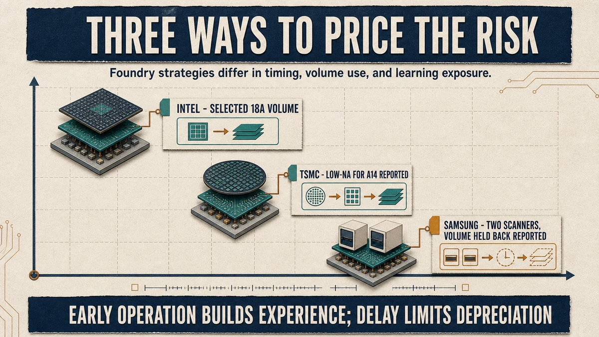
TSMC is reported to be skipping High-NA for A14, its 1.4 nm-class node due in 2028, and retaining 0.33-NA EUV with multi-patterning. Industry analysis cited in the published baseline suggests High-NA could raise lithography cost to about 2.5 times the alternative for the first sub-2 nm generation. A14P, around 2029, is described as a possible later point for reconsideration. TSMC is wagering that its existing multi-patterning expertise will produce a lower cost per good wafer than early High-NA adoption. It accepts more patterning complexity while avoiding the first wave of High-NA depreciation, utilization, and qualification risk.
Samsung is hedging. Supplied reporting says it took delivery of its first EXE:5200B in late 2025 and a second in the first half of 2026, buying two scanners for roughly $773 million combined. It reportedly expects to use High-NA on selected SF1.4 layers associated with 2029 mass production and could eventually have around seven systems. Yet other supplied reporting says Samsung was holding the machines back from high-volume operation to contain depreciation while working on its foundry turnaround.
Those facts imply that Samsung wants access without immediately paying the full cost of learning in volume. It reduces the risk of being unable to adopt High-NA later, but delayed operation can also delay the accumulation of defect, uptime, and overlay experience. Intel has taken the opposite side: accept utilization and execution risk earlier, then try to sell the resulting process confidence to customers.
ASML is positioned differently from every foundry. It sells the only High-NA platform described in the supplied material, and the baseline reports that it raised full-year guidance in the week of Intel’s milestone. ASML captures scanner revenue when a foundry adopts High-NA. It can also keep selling conventional EUV capacity when a foundry chooses multi-patterning. Zeiss optics and the specialist light-source supply chain participate in the adoption value, while the foundry customer carries the burden of turning installed capacity into economical wafers.
Downstream, fabless designers and hyperscalers including Nvidia, AMD, Broadcom, and cloud companies designing custom accelerators could gain from a credible second leading-edge foundry. The value would be pricing leverage, an alternative qualification path, and greater supply resilience for AI silicon. But those benefits exist only if Intel converts lithography readiness into a competitive process and external volume. A machine in Oregon is not yet a dual-source supply chain.
The claims the milestone cannot support
The headline invites conclusions the evidence does not carry. Shipping selected Panther Lake layers through High-NA does not make 18A a High-NA node. Most of the node is not described that way. It does not prove that High-NA is cheaper at full scale, because the economic comparison depends on layer selection, utilization, uptime, mask and etch savings, yield, and the depreciation absorbed by each good wafer.
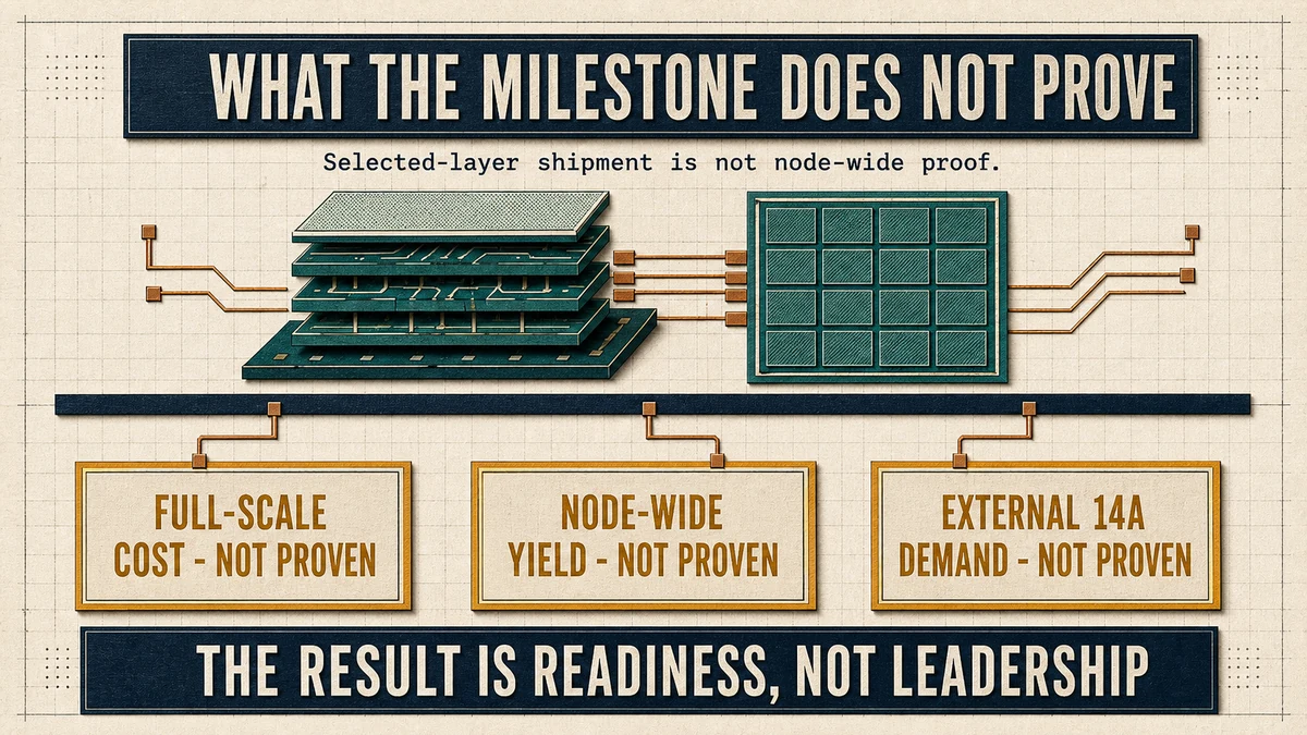
It does not establish node-wide yield superiority. Intel’s matched-yield statement concerns selected dual-qualified layers. The roughly 85% 18A yield is attributed to KeyBanc and is not an Intel disclosure. Combining the two into a claim that High-NA produced an 85% yield would be unsupported.
The milestone also does not land a committed external 14A customer. Reports of interest from large designers remain different from a named tape-out, qualification program, or volume agreement. Nor does the milestone close Intel’s overall foundry-share gap with TSMC. It buys experience and optionality. Customers still have to accept the design rules, qualify their designs, and believe Intel can deliver cost, performance, yield, and schedule together.
That negative space sharpens the central claim. This is not a Panther Lake win disguised as a lithography story. It is a 14A bet demonstrated through Panther Lake. The proof Intel has today is that High-NA can enter a shipping flow on selected layers with company-reported yield parity. The proof it still needs is that early learning changes the economics and adoption of the node where High-NA matters.
The checkpoints that decide whether Intel bought an advantage
1. The 14A PDK 0.9 release around October 2026. Supplied roadmap reporting identifies this as the design-rule lock that lets customers commit to tape-out. If it slips, Intel’s manufacturing learning loses schedule leverage because customer design work cannot advance on the expected timetable.
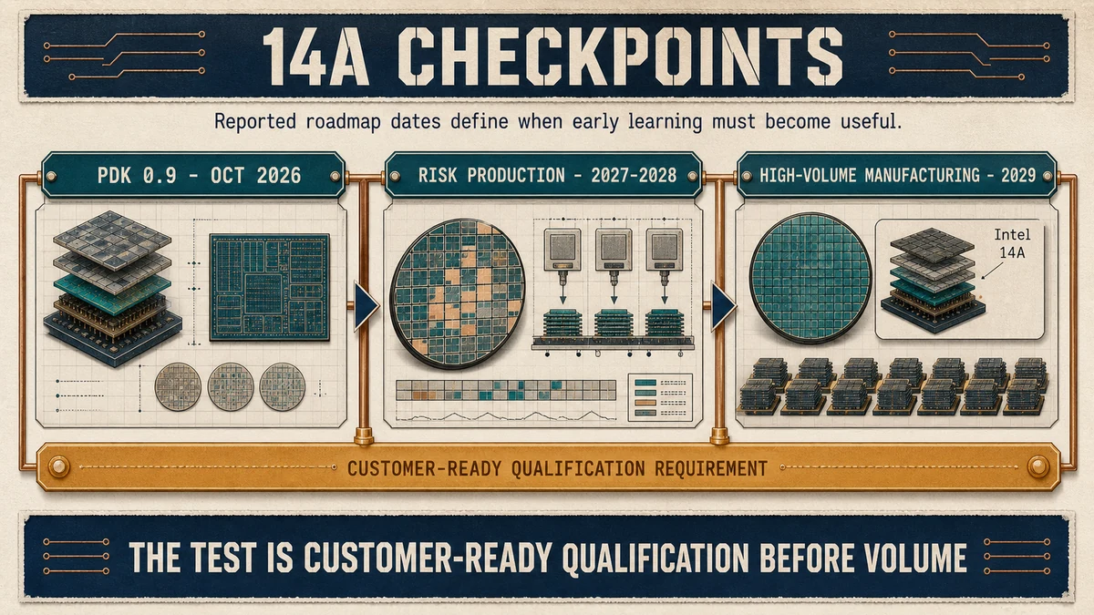
2. A named external 14A customer before 2028 risk production. The thesis requires conversion from technical readiness to demand. A disclosed tape-out or production commitment would matter. Unattributed interest would not settle it.
3. Evidence of competitive cost per good wafer. The relevant comparison is not scanner price alone. It is the High-NA route’s depreciation and operating cost against the masks, exposure time, overlay work, etch operations, cycle time, and yield loss of Low-NA multi-patterning. Intel wins only if the whole qualified flow is competitive.
4. Stable qualification beyond a few 18A layers. Intel needs repeatable uptime, overlay, defect, and yield performance as High-NA carries more process responsibility. A first shipment starts that record; it does not complete it.
5. TSMC’s A14 cost and A14P timing. If TSMC delivers A14 on Low-NA at competitive cost and waits until A14P in 2029, its restraint will look justified. An earlier move to High-NA would suggest that multi-patterning complexity reached its economic limit sooner than expected.
Strip away the first-place headline and what Intel bought is time: a chance to run the industry’s hardest lithography on real wafers before the node expected to depend on it. The tool is available to any foundry willing to pay. Qualified experience accumulates only through operation.
For Intel, the payoff is not Panther Lake itself. It is the possibility that two years of learning turn 14A from a roadmap promise into a credible external manufacturing option. For the AI economy downstream, the durable value would be a real dual-sourced leading edge rather than another isolated equipment milestone. Whether Intel earns that value turns on one number: how many external names sign onto 14A once the design rules lock.
This article is for informational and educational purposes only and does not constitute investment, financial, or legal advice.
Sources
- globenewswire.com — ASML/Intel: Intel Foundry first to ship high-volume logic with High-NA EUV; select 18A layers, Panther Lake, EXE:5200B, yields matched to NXE, exec quotes (2026-07-15)
- tomshardware.com — Confirms select Panther Lake 18A layers dual-qualified for 0.55-NA scanners, not the whole node (2026-07-15)
- techtimes.com — Reports KeyBanc’s estimate of roughly 85% 18A yield, up from about 65% in the prior quarter (2026-07-15)
- anysilicon.com — 14A PDK 0.5 shared; reported PDK 0.9 timing around October 2026; 14A-E timing (2026-07)
View all sources
- wccftech.com — TSMC reported to retain 0.33-NA multi-patterning for A14; reported cost concern and possible A14P timing (2026)
- trendforce.com — Samsung reportedly holding back High-NA volume use to contain cost while targeting selected SF1.4 layers (2026-07-17)
- tomshardware.com — Reported High-NA and standard EUV prices, EXE:5200B throughput, overlay, and 14A context (2026)
- morethanmoore.substack.com — Discussion of single-exposure High-NA, Low-NA multi-patterning, masks, etch steps, cost, and yield effects (2026-07)
- asml.com — ASML official product claims for EXE:5200B resolution, contrast, single-exposure scaling, density, and process complexity (2026)
- techtimes.com — Reports ASML’s full-year guidance increase in the week of Intel’s milestone (2026-07-15)
- techpowerup.com — Reports Samsung’s purchase of two High-NA scanners for roughly $773 million combined (2026)