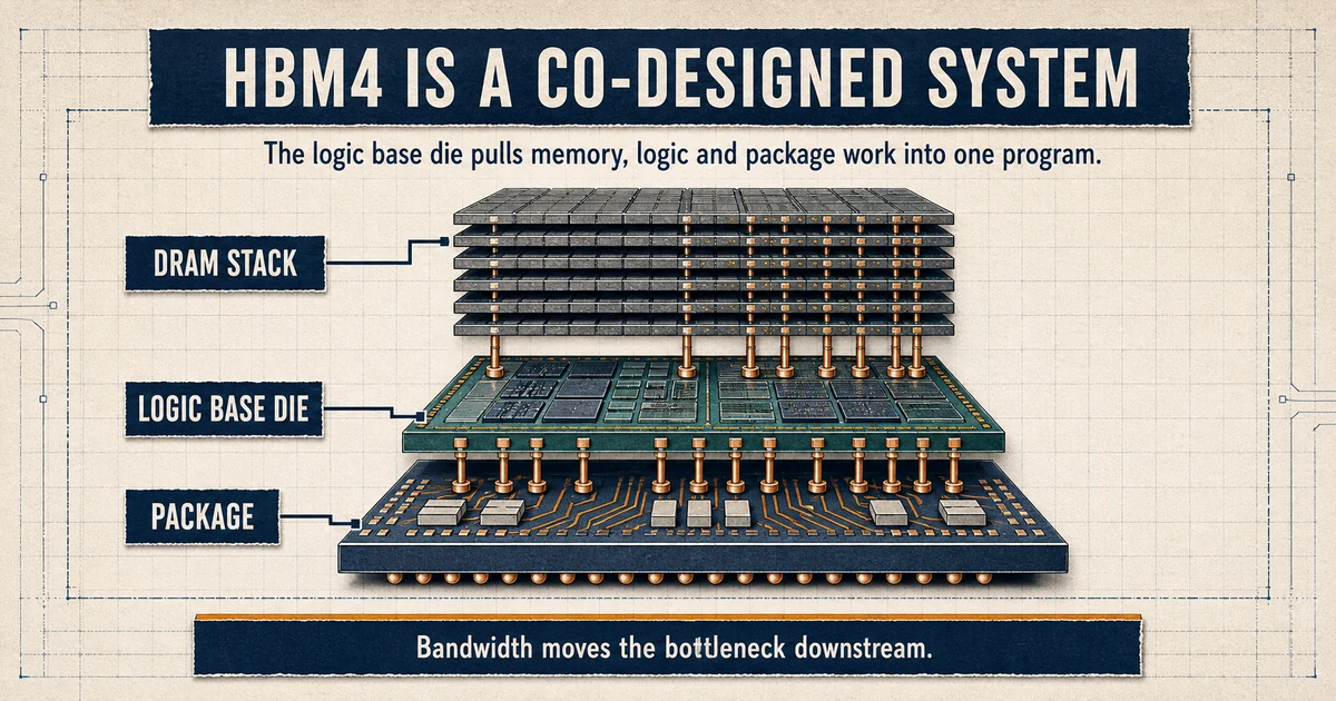
HBM4 is not merely another bandwidth generation. Its wider interface and more capable logic base die pull memory suppliers, foundries, packaging providers, and accelerator designers into one engineering program. The old boundary between standardized memory and custom logic does not disappear, but it moves downward into the base die and outward into the package.
High-bandwidth memory used to be described as stacked DRAM placed close to a processor. That description remains physically correct, but it no longer identifies the decisive engineering problem. In an HBM4 system, data must cross the DRAM stack, through-silicon vias, a logic base die, die-to-die links, an interposer, and a package while staying inside strict power, thermal, signal-integrity, and yield limits. Improving the DRAM cell is only one part of improving delivered accelerator performance.
The strategic change is the base die. It is becoming the point where foundry logic, customer requirements, memory design, power delivery, test functions, and packaging constraints meet. HBM4 is consequently less like a component selected after an accelerator is designed and more like a subsystem that must be specified before the accelerator and package are frozen.
This article examines that shift across the HBM4 system; a narrower companion analysis explains how custom HBM moves the bottleneck into base-die co-design.
Why 2,048 I/O connections make bandwidth a package result
HBM4 doubles the interface from 1,024 to 2,048 I/O connections. SK hynix, Samsung, and Micron all describe that wider interface in their HBM4 materials. At the 8 Gbit/s operating-speed baseline cited by SK hynix and Samsung for the JEDEC specification, the arithmetic is straightforward:
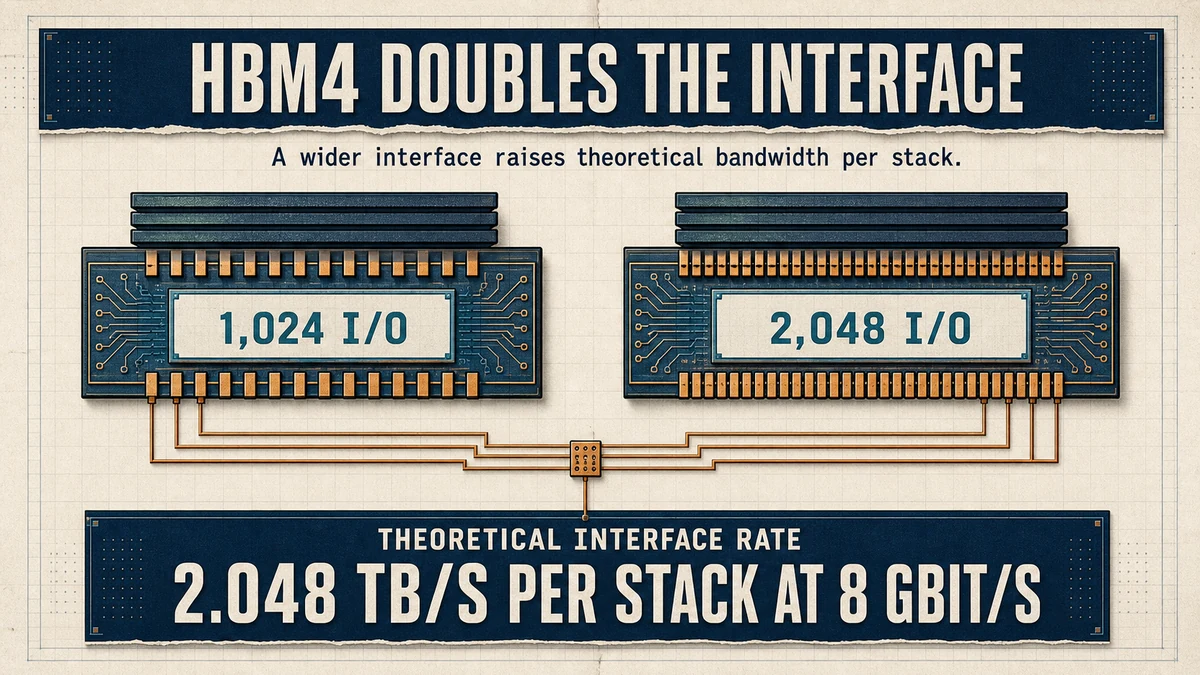
2,048 bits x 8 Gbit/s / 8 = 2,048 GB/s, or 2.048 TB/s per stack.
That theoretical interface rate is not an application benchmark. It does show the problem HBM4 is intended to remove: memory-interface bandwidth that cannot keep pace with accelerator demand. Yet twice as many data paths must also be routed, powered, tested, and held within timing and thermal limits. The package has to deliver the bandwidth without surrendering too much of it to clock constraints, congestion, heat, repair overhead, or system inefficiency.
Supplier announcements show why “HBM4 speed” is not one number. SK hynix says its HBM4 operates above 10 Gbit/s. Micron specifies more than 11 Gbit/s and more than 2.8 TB/s per stack. Samsung says its commercial HBM4 sustains 11.7 Gbit/s and can reach 13 Gbit/s. The same interface calculation puts 11.7 Gbit/s near 3.0 TB/s and 13 Gbit/s near 3.3 TB/s.
Those figures are company claims covering different configurations and test conditions, not results from one independent benchmark. A buyer still needs delivered bandwidth at operating temperature, energy per transferred bit, stack and package yield, repair behavior, capacity per accelerator, and qualification results with a specific compute die. A faster stack that destabilizes the package or reduces manufacturing yield can create less system value than a slower but repeatable design.
The logic base die redraws the memory-foundry boundary
Until HBM3E, SK hynix says it used its own proprietary process for the base die. In its 2024 partnership announcement with TSMC, the company said it would use TSMC logic technology for HBM4 so additional functionality could fit into the limited base-die area. The announcement described the operating model explicitly: product design, foundry, and memory working together.
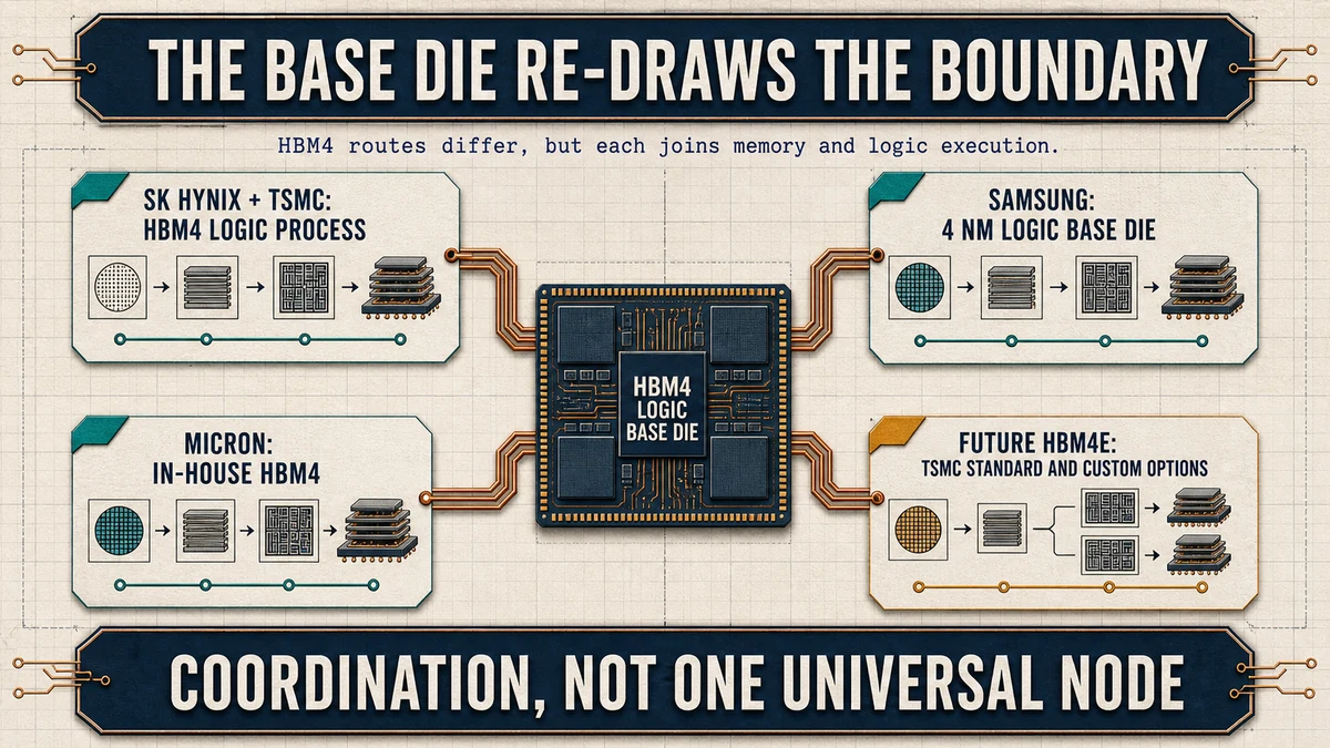
TSMC has provided a distinction that prevents a common reporting error. The foundry identified N12 for HBM4 logic base dies and N3P for custom HBM4E designs. These are not interchangeable descriptions of one product. Calling every HBM4 base die “3 nm” or “4 nm” collapses a standard implementation, supplier-specific choices, and a customized HBM4E roadmap into one misleading label.
Samsung demonstrates another route. Its shipping HBM4 combines 1c DRAM with a 4 nm logic base die, according to the company. Samsung argues that coordination among its memory, foundry, and advanced-packaging operations improves design-technology co-optimization and production responsiveness. That is an organizational advantage in principle, not proof of superior customer yield.
Micron shows why the boundary is not moving in only one direction. Its current HBM4 materials describe an internally designed and manufactured logic base die, while the company’s investor presentation says future HBM4E will include standard and customized base-die options manufactured with TSMC. The market is not converging on one vertical-integration model. It is converging on the need to coordinate memory and logic processes, whether the work occurs inside one company or across contractual boundaries.
| Supplier strategy | Publicly described base-die route | What still needs proof |
|---|---|---|
| SK hynix + TSMC | TSMC logic process for HBM4; N12 and future custom HBM4E direction | Qualification speed, package yield, and repeatable customer ramps |
| Samsung | 1c DRAM, 4 nm logic base die, internal foundry and packaging coordination | Whether integration produces better yield and lead time across customers |
| Micron | In-house logic for current HBM4; standard and customized TSMC-made HBM4E options | Custom-volume share and the realized margin and yield trade-off |
The new bottleneck is joint execution across the package
Moving logic into the base die can improve interfaces, power management, test, and workload-specific behavior. It can also reduce data movement if useful functions are placed closer to memory. But every capability consumes area and power, adds verification work, and tightens dependencies on the rest of the package.
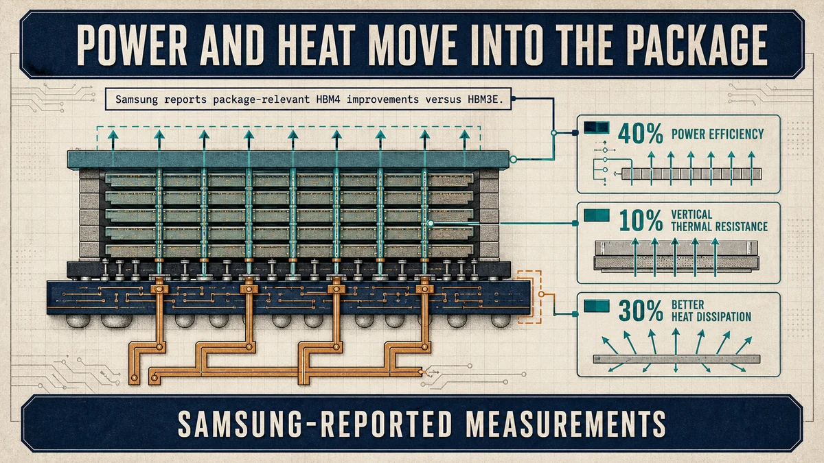
Samsung’s HBM4 announcement acknowledges that doubling the I/O count creates power and thermal challenges. The company reports a 40% improvement in power efficiency, a 10% improvement in vertical thermal resistance, and 30% better heat dissipation relative to HBM3E. These figures are useful design targets, but they remain company measurements until aligned test conditions and independent results permit direct comparison.
Package scale is moving at the same time. TSMC’s 2025 Technology Symposium material says a 9.5-reticle CoWoS platform planned for volume production in 2027 will support 12 or more HBM stacks with leading-edge logic. More stacks increase capacity and aggregate bandwidth, but they also expand routing, power-delivery, warpage, thermal, and known-good-die problems. The next constraint may be interposer size, package assembly throughput, substrate supply, cooling, or the ability to identify failures before expensive components are combined.
Semiconductor Engineering reports that HBM4 retained microbumps rather than moving immediately to hybrid bonding after JEDEC increased the permitted module height. Its interviews cite cost, test access, surface cleanliness, equipment, and yield as reasons to postpone the denser interconnect. The decision is a useful counterexample to a simple “newest process wins” story. Process maturity and inspectability can outweigh a theoretically superior connection technology for one generation.
The same discipline matters beyond HBM: an advanced-packaging yield number changes meaning with the process step being measured.
The bottleneck migration
– The 2,048-bit interface relieves memory-interface bandwidth pressure.
– The logic base die makes foundry execution part of memory differentiation.
– Package power, heat, test, yield, and customer qualification become the downstream constraints.
This is the semiconductor pattern that matters: a technology removes one bottleneck and creates another downstream. HBM4 transfers risk from the memory interface into base-die design, package integration, cooling, production coordination, and qualification. The current bottleneck is the coalition’s ability to make all of those interfaces work together at volume.
Custom HBM reallocates value, cost, and schedule risk
Standard memory spreads design cost across many customers. Inventory can be redirected when one program slows, while qualification centers on a common interface plus supplier-specific performance. A customer-specific base die changes that economic contract.
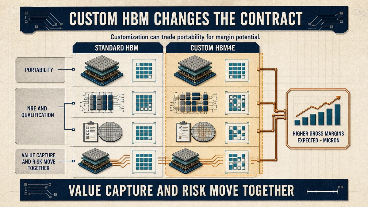
Customization adds non-recurring engineering, masks, physical verification, firmware and test work, and customer-specific qualification. It also links the memory schedule more tightly to accelerator and package schedules. If the accelerator slips or its volume forecast falls, a customized HBM part may be difficult to redirect. If a quality problem appears, changing suppliers requires reproducing electrical, thermal, test, firmware, and manufacturing behavior, not merely matching a datasheet bandwidth figure.
The potential value is equally concrete. Workload-specific logic can improve system efficiency, and long co-development programs can make demand more visible. Micron told investors that it expects customized HBM4E base dies to generate higher gross margins than standard products. That is a company expectation, not observed profitability, but it shows that suppliers see customization as a change in value capture rather than a free technical option.
The value and risk do not sit with one participant. Memory suppliers can gain margin and tighter customer relationships, but they accept engineering, inventory, concentration, and yield exposure. Foundries capture logic work while owning process execution and schedule dependencies. Packaging providers own assembly throughput, inspection, and integration performance. Accelerator vendors may gain workload efficiency, but they also absorb qualification, switching, and program-delay risk.
The market is therefore likely to remain segmented. Accelerator vendors and hyperscalers with stable, very large volume can amortize custom design and qualification. Smaller customers may prefer standard HBM because portability and inventory flexibility are more valuable than the last increment of optimization. The dividing line is whether expected system savings exceed custom engineering, masks, qualification, yield loss, and concentration risk.
Standard base-die volume remains the decisive market test
HBM4 does not automatically erase the memory-foundry boundary. The JEDEC HBM4 standard still creates a common interface, and standardized DRAM core dies remain central. The stronger claim, that custom logic turns HBM into a co-designed system, should be treated as a hypothesis with measurable failure conditions.
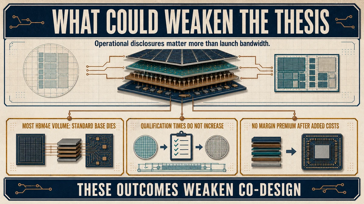
The thesis weakens if most HBM4E volume remains on standard base dies, accelerator qualification times do not increase, or customers can switch suppliers without redesigning the package and firmware. It also weakens if customized products fail to deliver a margin premium after lower yield, extra masks, engineering support, and customer-specific inventory are included.
The next 12 to 24 months should therefore be judged by operational disclosures, not launch bandwidth:
- the share of HBM4E programs using customer-specific base dies;
- base-die, stack, and final-package yield at volume;
- time from first silicon to accelerator qualification;
- energy per delivered TB/s at realistic temperature;
- package assembly throughput and known-good-die escape rates;
- inventory that can be reassigned when a customer schedule changes;
- realized gross-margin differences between standard and custom HBM;
- whether second-source qualification remains practical.
HBM4 is often framed as a race among memory vendors. If the co-design thesis holds, the more accurate unit of competition will be the engineering coalition around each accelerator, not the vendor with the fastest DRAM or the smallest logic node in isolation. The advantage exists only when the coalition can co-design memory, base-die logic, package, power, cooling, test, and customer qualification, then manufacture the combination at repeatable yield.
This article is for informational and educational purposes only and does not constitute investment, financial, or legal advice.
Sources
- news.skhynix.com – SK hynix said it would use TSMC logic technology for the HBM4 base die. (2024-04-19)
- semiconductor.samsung.com – HBM4 doubles the interface width from 1,024 to 2,048 I/O connections.
- investors.micron.com – Micron expects customized HBM4E base dies to have higher gross margins than standard HBM4E. (2025-09-23)
- jedec.org – HBM4 doubles the interface width from 1,024 to 2,048 I/O connections.
View all sources
- news.skhynix.com – HBM4 doubles the interface width from 1,024 to 2,048 I/O connections.
- tsmc.com – TSMC identified N12 for HBM4 logic base dies and N3P for custom HBM4E.
- pr.tsmc.com – TSMC plans a 9.5-reticle CoWoS platform for 2027 supporting at least 12 HBM stacks.
- micron.com – HBM4 doubles the interface width from 1,024 to 2,048 I/O connections.
- semiengineering.com – HBM4 retained microbumps as cost, test access, and yield delayed broad hybrid-bonding adoption. (2026-01-13)