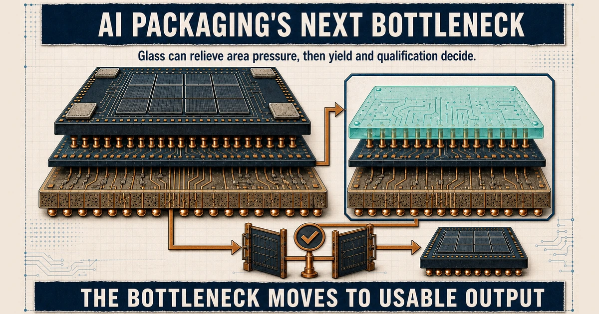
At ECTC 2026, Intel Foundry reported that fully copper-filled through-glass vias “withstand severe thermal cycling without failure, confirming long-term reliability”. The same week, from the same conference floor, an independent observer recorded that STATS ChipPAC’s 74 mm x 74 mm glass-core packages failed every test segment without edge coating.
Both reports are accurate. One is measured on a hole. The other is measured on a finished package with dies mounted on it. Between them sits the routed substrate, which is where most published glass results actually live.
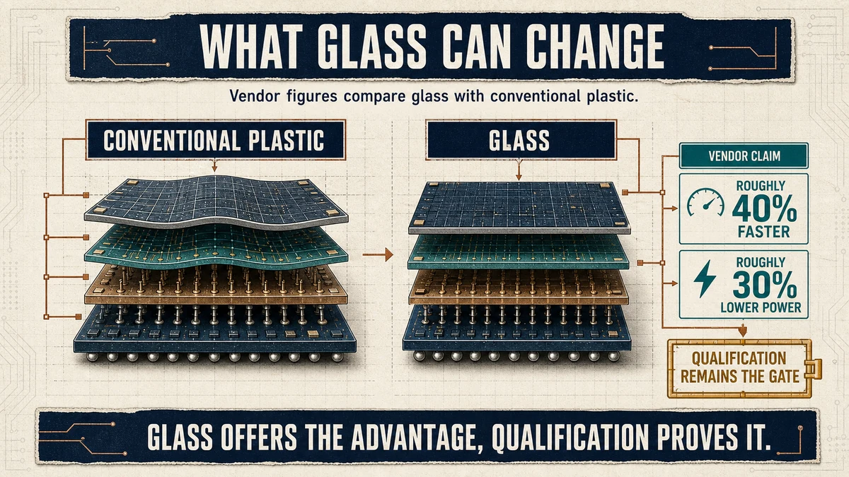
That gap is the whole commercial question. Glass has real advantages, and they are not seriously contested: Intel claims a 10x increase in interconnect density is possible on glass, along with 50% less pattern distortion and the dimensional stability needed for tight layer-to-layer overlay. Those are vendor figures, and they describe the material. What decides whether AI packages ship on glass is whether anyone can drill, metallize, inspect and assemble it at high yield – and the word yield, in the 2026 record, refers to at least three different numbers that nobody labels.
Three places to measure the same word
Sort the 2026 results by the step at which each was measured rather than by the date it was announced, and the direction reverses as you climb.
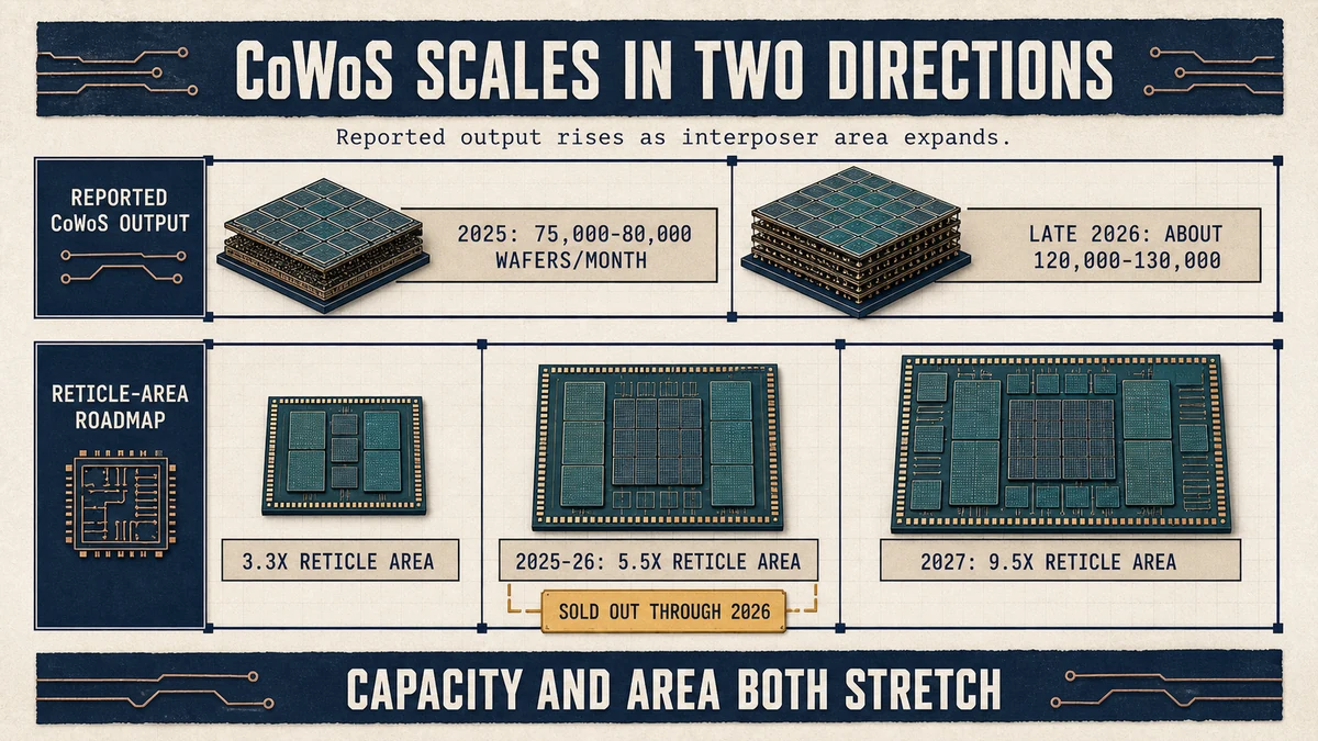
At the via, glass passes. Intel Foundry’s copper-filled TGVs survived severe thermal cycling without failure, measured on the vias themselves.
At the substrate, glass passes. Intel demonstrated a 510 mm x 515 mm, 24-layer glass-core panel with fully copper-filled TGVs, two embedded EMIB bridges and optical waveguides co-formed between the vias; it was processed on existing organic-substrate lines, and singulated units showed no cracking after thermal shock testing. Six months earlier the company had shown a first EMIB-plus-glass-core sample with no micro-cracks at NEPCON Japan. As adopters, Amkor and STATS ChipPAC measured 30-40% lower substrate-level warpage with a thinner glass core than with their organic references.
At the completed package, it does not. The same floor report that recorded the panel also recorded severe warpage in the sample on display, along with assembly defects and TGV filling problems, and concluded that this year’s data support manufacturing development rather than high-volume adoption. STATS ChipPAC’s 74 mm x 74 mm packages failed every test segment without edge coating; adding the coating reduced warpage by 33.5% relative to the uncoated package.
The step that rescued that result is an assembly process owned by the packaging house, which means the pass is not explained by the quality of the glass alone.
At the production line, the one disclosure available points the same way. BOE’s glass substrate pilot line has a design capacity of 1,000 panels per month, and the same disclosure states that this figure “cannot be treated as current shippable good-unit capacity” and that “the pilot line’s yield has not yet reached mass-production levels”. Trade coverage independently dates the shortfall. Neither disclosure names which process step is responsible.
None of these numbers can substitute for another, and among the 2026 sources examined here, no supplier publishes a yield figure with its measurement boundary attached. Two suppliers could therefore quote figures that appear to contradict each other while both describe their own results correctly.
The failure happens inside tens of thousands of holes
Glass evokes breakage, and Intel’s own account puts handling before physics: “the whole substrate industry has to remap to be able to handle the glass”, with open questions about edge cracking, singulating a sheet full of substrates, and moving them through a factory at all. The manufacturing problem is quieter than that, and it sits inside the vias.
Each formation route leaves its own defect signature. A peer-reviewed survey reports that abrasive jet machining leaves an inner wall around 1.6 um rough that takes a conical shape, laser ablation produces heat-affected zone expansion and protrusions near via edges that impede bonding, and electrochemical discharge machining leaves its own heat-affected areas that affect reliability; vias with aspect ratios over 10 are difficult across every method.
Metallization compounds it. Improper electroplating parameters produce voids, incomplete filling or discontinuous columnar structures inside the vias; uneven filling varies hole resistance; copper diffusion into the glass degrades insulation over time; and the large CTE difference between copper and glass accumulates thermal stress until the interface delaminates. Brittleness then converts any microcrack introduced during processing, packaging, testing or use into an electrical anomaly. As one industry account puts it, there cannot be any mistakes in the tens of thousands of holes.
So the cost lands on inspection. Screening has to measure the critical dimension at the top, waist and bottom of each via plus its positional accuracy against the design, and detect microcracks along individual TGVs, incomplete etching, over- and under-plating, polishing variation and surface roughness. In auxiliary commentary from Mark Lapedus (Semiconductor Insights), one inspection-equipment maker self-reports a detection accuracy of 1.75 um at the laser phase and 3.5 um post-etch for its own tools – a single vendor’s self-reported capability, not an industry specification.
That is a separate fact from panel size: a different via-formation equipment vendor states its tools are compatible with panel formats up to 600 x 600 mm, which says nothing about whether the first vendor’s inspection accuracy holds at that scale.
One consequence travels badly. Because each formation route produces a different defect population, an inspection limit qualified on one supplier’s vias is not evidence about another’s. A yield figure depends on the process route as well as on the measurement step.
The deciding step does not belong to the glass maker
Look at where each 2026 result was actually won or lost, and the owner changes each time. The package-level failure was reversed by edge coating, a packaging-house process. The pilot-line shortfall is a line result whose cause is undisclosed. The most detailed public account of what inspection requires comes from a metrology vendor.
Public disclosure is thinnest at the equipment and inspection steps. LPKF, whose laser-induced deep etching is used to form TGVs, states that more than 80% of customers among major global players have selected its equipment, that adoption is moving beyond process validation toward mass-production readiness, and that orders began to materialize in the first quarter. Its glass-core page claims “process stability for high yield and repeatability” and publishes no yield number, no via dimension and no throughput figure. The non-disclosure pattern repeats at the equipment step, not only at the substrate step.
Intel’s 2026 collaboration with Lens Technology is scoped the same way. The public release announces cooperation on critical manufacturing processes without naming a volume, a timeline or a location. The counterparty’s own exchange announcement is stricter: what Intel contributes is illustrative architecture information, design-for-manufacturability guidelines, benchmarking methods and verification methods; every item requires a separate written agreement; and the document reflects preliminary intent. The memorandum runs one year, does not commit either party to any transaction or commercial outcome, and leaves process verification, product qualification and mass production to contracts not yet signed.
The one concrete commitment in the announcement belongs to the partner: a 30,000 square metre dedicated glass substrate plant due into service by the end of the year.
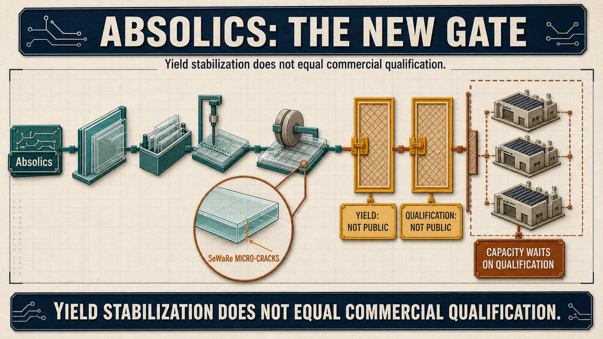
Korean suppliers sit on the same ladder. Samsung Electro-Mechanics was running prototype performance verification with global customers on its Sejong pilot line in March, and in July agreed a glass core joint venture with Dongwoo Fine-Chem worth roughly KRW 480 billion, split 66/34, with full-scale operations scheduled for the second half of 2027. Absolics has completed substrate-level reliability testing at its Georgia fab and preliminary electrical characterization in Japan, and package-level reliability evaluation in Taiwan had only just begun as of late July.
Its public site carries platform language and CHIPS subsidy amounts and states no panel size, no production volume, no sampling status and no customer names. SKC, the parent, said in February that commercialization is running behind market expectations because unforeseen additional validation items keep extending development, and that it cannot fix a shipping date. The constraint it names is an accumulating list of customer validation items.
Everyone with something to build is pointing at 2027 and 2028
Collect the dated readiness statements and group them by where the speaker sits in the chain. The equipment vendor LPKF says full-scale mass production starts in 2027. TSMC plans a pilot line at VisEra this year, trial production in 2027 and mass production in the second half of 2028. Secondary reporting from IndexBox – not SEMI and Global Net Corp.’s own document – puts initial production around 2028 in specific high-performance applications.
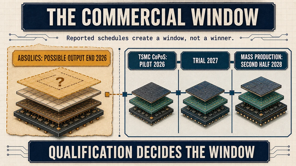
Trade coverage points the same direction, at one remove: Mark Lapedus (Semiconductor Insights), writing in the same newsletter cited above for inspection accuracy, expects small batches as early as 2027 and relatively stable capacity in 2028 – his own commentary read, not an official vendor forecast, and one that names no supporting data or customers. The Korean joint venture reaches full-scale operation in the second half of 2027, and SKC will not name a date at all.
Five vantage points that do not share a source – an equipment maker, TSMC, IndexBox’s secondary reporting of SEMI and Global Net Corp., a trade newsletter, and the Korean joint venture – land inside the same two-year window, and none of them is 2026.
The prize is smaller than the headline forecasts imply, too. Yole’s best case puts glass core substrate revenue at $275 million by 2030, while a widely quoted $8.1 billion by 2030 covers FO-PLP and glass substrate together. Those figures do not conflict; they have different denominators, which is the same disclosure failure that yield numbers carry.
On this evidence, the reasonable expectation is selective adoption first, in large premium AI and high-performance-computing packages where routing density and package size already constrain roadmaps and a failed package is expensive to lose. That is an inference from where the qualification activity is concentrated, not a schedule anyone has published.
Yield, Not Arrival Order, Was Always the Constraint
An earlier instalment on this site argued that AI packaging’s bottleneck had moved from the chip to the surface beneath it, and that for once the supplier closest to commercial scale on that surface was a merchant fab rather than the foundry that owns the current one, with yield rather than demand named as the binding constraint. That caveat turned out to be the whole story, and it is sharper than “yield is hard”.
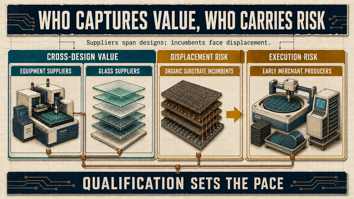
The 2026 record reports the same technology winning at the substrate step and failing at the package step inside a single season, which means the word yield does not name one number. Which supplier arrives first matters less than which step any of them is measuring when it quotes a figure – and on that earlier question the race is still open, with Absolics only now beginning package-level evaluation and Samsung Electro-Mechanics still at prototype verification as of March.
Perspective
That reading is falsifiable on a specific observation: a yield published on completed packages after die attach at a level a customer would buy, or a named accelerator shipping in volume on a glass core before 2028. Either would move the question back from measurement discipline to schedule.
Bottom Line
The materials case for glass is largely settled and largely published by the companies that benefit from it. What is missing from the 2026 record is a yield figure with its measurement boundary stated – bare core, routed substrate, or completed package after die attach – and without that label, the same technology reads as a success at the via and a failure at the package without anyone misstating a result. Whether a supplier states the boundary when it publishes its first figure is itself informative, though only alongside the sample size and the completion stage that figure covers.
Sources
- newsroom.intel.com — Intel’s vendor claims for glass: 10x interconnect density, 50% less pattern distortion, dimensional stability for tight layer-to-layer overlay, and delivery in the second half of the decade. (2023-09-18)
- newsroom.intel.com — Intel’s own handling agenda: the substrate industry must remap to handle glass, with edge cracking, singulation and factory transport listed as open questions. (2023-11-16)
- newsroom.intel.com — The Intel-Lens Technology announcement, which names no production volume, no manufacturing timeline and no facility location. (2026-07-24)
- xenospectrum.com — The memorandum’s one-year term and non-commitment clauses, and BOE’s pilot line at 1,000 panels per month of design capacity with yield below mass-production levels and no shippable good-unit figure. (2026-07-29)
View all sources
- newsletter.semianalysis.com — First-hand ECTC 2026 observations: the 510 x 515 mm 24-layer panel and its thermal-shock result, severe warpage in the displayed sample, STATS ChipPAC’s 74 x 74 mm packages failing every test segment without edge coating, the 33.5% warpage reduction from edge coating, and 30-40% lower substrate-level warpage at Amkor and STATS ChipPAC. (2026-07-02)
- istgroup.com — Through-glass via failure modes: plating voids and discontinuous columns, hole-resistance variation from uneven fill, copper diffusion, CTE-driven interface delamination, and microcrack-induced electrical anomalies. (2025-09-09)
- ontoinnovation.com — The per-via metrology load – CD at top, waist and bottom plus positional accuracy, microcracks, plating and polishing variation – and Yole’s best-case $275 million glass core substrate revenue by 2030. (2025-10-06)
- marklapedus.substack.com — Auxiliary commentary from Mark Lapedus (Semiconductor Insights): the tens-of-thousands-of-holes framing, an equipment vendor’s self-reported inspection detection accuracy of 1.75 um at the laser phase and 3.5 um post-etch, and Lapedus’s own unsourced expectation of small batches in 2027 with stable capacity in 2028 – commentary, not an official vendor forecast. (2026-01-06)
- lcdproduct.com — Independent dating of BOE’s glass packaging substrate line remaining short of mass production. (2026-06-05)
- thelec.net — Absolics’ qualification ladder: substrate-level reliability at the Georgia fab, electrical characterization in Japan, and package-level reliability evaluation only beginning in Taiwan. (2026-07-27)
- greened.kr — SKC on the record that commercialization is running behind market expectations because unforeseen additional validation items keep extending development, with no shipping date fixable. (2026-02-06)
- epnc.co.kr — Samsung Electro-Mechanics running prototype performance verification with global customers on its Sejong pilot line, and Absolics building in Georgia ahead of Intel. (2026-03-30)
- insights.trendforce.com — Intel’s first EMIB-plus-glass-core sample at NEPCON Japan in January 2026, achieving no micro-cracks. (2026-05-05)
- absolicsinc.com — Absolics’ public disclosure profile: platform language and CHIPS subsidy amounts, with no panel size, production volume, sampling status or customer names. (2026-08-06)
- cls.cn — Lens Technology’s exchange announcement: Intel contributes architecture information, DFM guidelines, benchmarking and verification methods; every item requires a separate written agreement; the partner’s own 30,000 sqm plant is the one concrete commitment. (2026-07-24)
- trendforce.com — The Samsung Electro-Mechanics and Dongwoo Fine-Chem glass core joint venture: roughly KRW 480 billion, 66/34 ownership, full-scale operations in the second half of 2027. (2026-07-06)
- thelec.net — TSMC’s VisEra pilot line, 2027 trial production and 2H 2028 mass production, and the $8.1 billion by 2030 forecast covering FO-PLP and glass substrate combined. (2026)
- indexbox.io — IndexBox’s secondary reporting of a SEMI and Global Net Corp. forecast, not SEMI’s own document, placing initial production around 2028 in specific high-performance applications. (2026-05-27)
- lide.lpkf.com — LPKF on full-scale mass production from 2027, over 80% of major global players selecting its via-formation equipment, compatibility up to 600 x 600 mm, and a high-yield claim with no yield number published. (2026-08-06)
- indexbox.io — Intel Foundry’s own ECTC 2026 account: fully copper-filled TGVs withstand severe thermal cycling without failure, measured at the via. (2026-06-01)
- pmc.ncbi.nlm.nih.gov — Peer-reviewed TGV survey: formation-route-specific defect signatures (1.6 um wall roughness and conical vias, laser heat-affected zones and edge protrusions, ECDM thermal damage) and the aspect-ratio-over-10 limit. (2024-01-01)
This article is for informational and educational purposes only and does not constitute investment, financial, or legal advice.