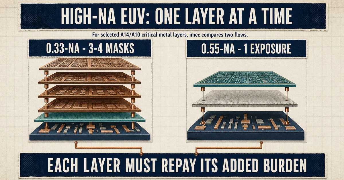
High-NA EUV will not replace conventional EUV across a process by default. Its value depends on whether improved resolution removes enough patterning steps, defect opportunities and cycle time on a particular layer to repay the tool and ecosystem cost.
Lithography transfers circuit patterns onto a wafer. The current economic bottleneck appears when shrinking features force manufacturers to divide one layer across multiple exposures and processing steps on 0.33-NA EUV equipment. That extends a known flow, but it also adds masks, alignment work, deposition and etch operations, cycle time and defect opportunities. High-NA EUV raises numerical aperture to 0.55, improving resolution and image contrast. The consequential question is not whether it prints a smaller pattern. It is whether removing multipatterning on a particular layer creates more value than the new equipment, materials, field and qualification burdens consume.
High-NA EUV is a layer-by-layer P&L decision
The useful unit of analysis is the layer, not the node. imec’s review of High-NA EUV presents 0.55-NA as a route to dimensional scaling, process simplification and design flexibility, while stressing that materials, masks, metrology, inspection and design must be co-optimized. For selected A14 or A10 critical metal layers, imec reports that a 0.33-NA flow can require three or four masks while a 0.55-NA exposure can print the comparable structure in one exposure. This is a reported process-flow comparison for selected layers, not a promise for every layer in a node.
The problem potentially removed is expensive multipatterning. The local test is whether avoided masks, exposures, etch operations and alignment steps, plus any yield and cycle-time benefit, exceed the added scanner, resist, mask, metrology, inspection, power and qualification cost. A layer that removes three masks may clear that hurdle. One that gains resolution but creates a dose penalty, inspection queue, stochastic-defect problem or stitching risk may not.
The bottleneck moves rather than disappears. A previous HBM package analysis traced a bandwidth constraint into package qualification, while a glass-substrate packaging analysis traced a materials change into cost and certification risk. High-NA follows the same pattern: optical resolution can remove a patterning constraint, then move the burden into image fidelity, field coverage, materials behavior and process control.
Resolution does not arrive alone
Higher NA changes the imaging system, but the scanner is only one part of the manufacturing result. Anamorphic optics reduce the exposure field in one direction, affecting die and mask planning. Resists must resolve smaller features without unacceptable roughness or stochastic defects. Masks, pellicles, metrology, inspection, etch and computational lithography must mature together. The scanner removes one optical boundary while creating a broader integration boundary.
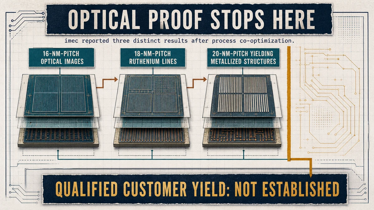
The experimental distinction matters. imec has reported 16-nm-pitch optical images, 20-nm-pitch yielding metallized structures and 18-nm-pitch ruthenium lines after process co-optimization. Its High-NA ecosystem overview frames early adoption as a materials, mask, etch and metrology challenge rather than a scanner-only upgrade. An optical image demonstrates imaging capability. It does not establish manufacturing yield, because resist, underlayer, etch, mask, inspection and wafer-level variability still have to survive together.
Throughput sits on the same boundary. A high-resolution exposure that requires a slower dose or creates an inspection queue may not lower cost. Conversely, removing deposition, etch and clean steps can shorten the route enough to justify a more expensive scanner. Tool price divided by wafer starts is therefore an incomplete comparison. The relevant measure is cost per good die or good wafer, including yield, throughput, qualification time and the capital tied up across the full process sequence.
Early adoption will target expensive complexity
Not every layer needs maximum resolution. Some patterns remain efficiently printable with conventional EUV or deep ultraviolet lithography. High-NA should first appear where multipatterning is most complex, overlay-sensitive or cycle-time intensive. A manufacturer can insert it on a limited set of critical layers and expand only after operating data shows where the new flow is reliably better.

Value and risk are distributed unevenly. ASML and the surrounding mask, resist, inspection and metrology suppliers can capture value from a larger equipment and materials ecosystem. Foundries own the integration task and bear the near-term utilization, qualification and yield risk. Fabless customers benefit only if the foundry converts the capability into competitive performance, schedule and cost per good die.
Only a small group of manufacturers can buy these systems, but ownership is not mastery. Engineers still need stable defect control across interacting optics, resist, mask, metrology and etch choices. Development-line learning can shorten a later ramp; premature insertion can consume capital without improving customer output. Useful indicators include representative wafers processed, overlay and defect distributions, resist readiness, tool availability, qualification time and the number of process steps actually removed.
The field shrinks while the process expands
High-NA’s anamorphic optics expose half the conventional EUV field in one direction. Large-die coverage thus becomes a manufacturing decision rather than a layout detail. Semiconductor Engineering’s reticle analysis describes two broad responses: stitch exposures accurately or move toward a larger mask format that would require a major change to mask infrastructure.
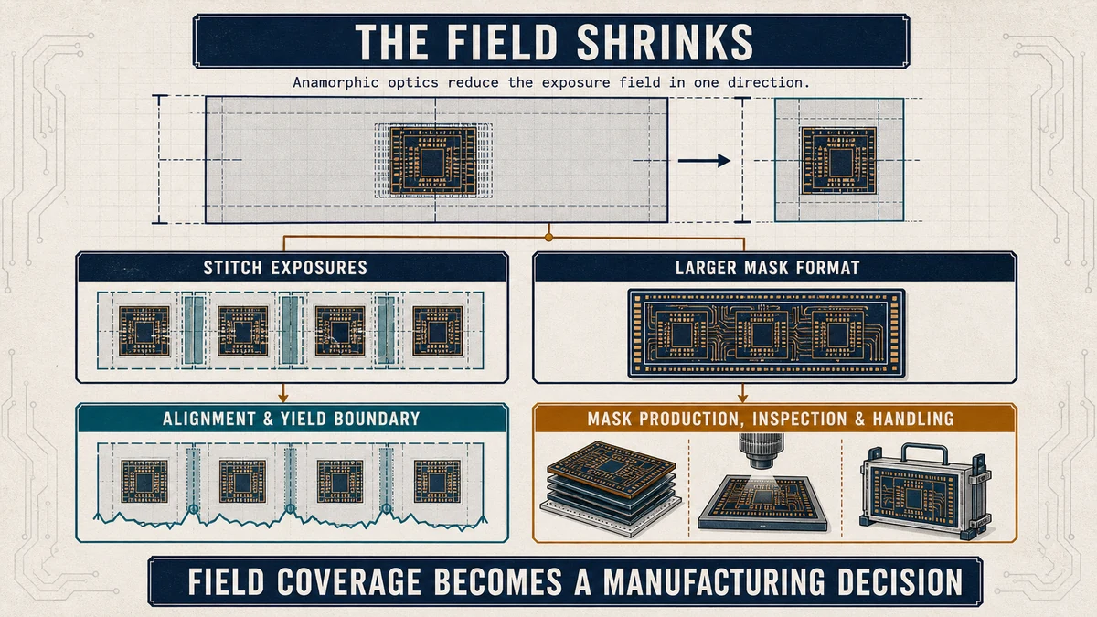
Stitching can preserve the current mask ecosystem, but it adds an alignment and yield boundary. Larger masks can recover productivity, but they move capital and qualification work into mask shops, inspection and handling. The right choice depends on die size, volume and the share of the process that uses High-NA. Chiplets can reduce the field problem, but they may move cost and risk into packaging, interconnect and system integration.
The process becomes more demanding in less visible ways. Semiconductor Engineering’s mask-economics review reports tighter requirements for critical dimension, edge-placement error, local CDU, mask 3D effects, stitching and materials. Reduced depth of focus makes resist thickness and profile control more sensitive. A simpler exposure count can therefore create a longer materials and qualification loop.
The equipment milestone is not a manufacturing verdict
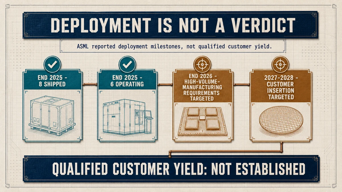
ASML’s 2025 annual report records the first full-specification TWINSCAN EXE:5200B delivery to a customer and presents 0.55-NA EUV as a route to simplify multipatterning. Its 2026 AGM presentation says eight High-NA systems had shipped by the end of 2025, six were operating, and the company was targeting high-volume-manufacturing requirements by the end of 2026 with customer insertion in 2027-2028. These are company-reported deployment milestones. They do not establish qualified customer yield or cost per good die.
Intel’s High-NA announcement says it expects to use both 0.33-NA and 0.55-NA EUV alongside other patterning processes, beginning with 18A proof points and continuing into 14A production. Its 18A platform brief provides design-technology integration context for that roadmap. Intel’s earlier High-NA 14A analysis explains why this is a roadmap choice rather than proof that every 14A layer will use High-NA or that it will be cheaper for every customer.
Early access can build process knowledge and influence tools, resists and metrology. An installed scanner is still only the starting point. Manufacturers must demonstrate stable defect control across interacting process parameters and repeat that result at commercially useful throughput. Later insertion is not automatically technological weakness if an optimized multipatterning flow remains more economical on the selected layers.
Cost per good wafer decides which layers adopt High-NA
The thesis fails under three conditions. First, High-NA layers do not remove enough masks and process steps to offset scanner and ecosystem cost. Second, stitching, stochastic defects or reduced depth of focus create a qualification burden larger than the avoided multipatterning burden. Third, large-die products cannot recover the field-size penalty through design partitioning, stitching control or mask investment.
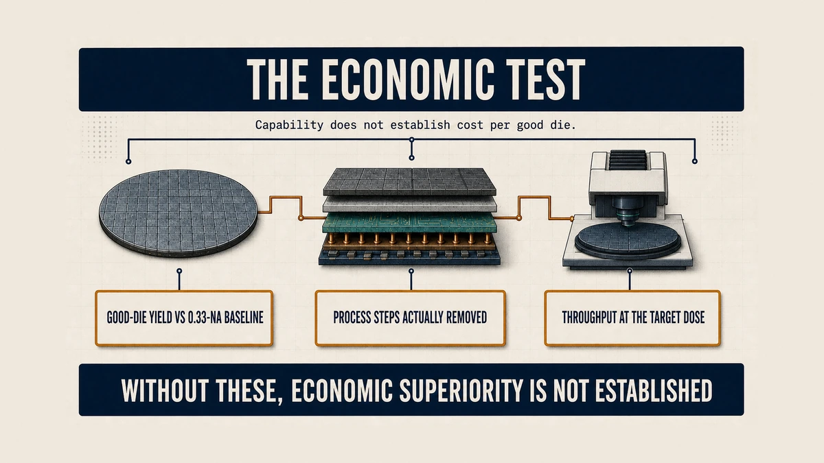
The next useful disclosures are concrete: good-die yield against the 0.33-NA baseline; masks, deposition operations and etch steps actually removed; overlay and defect distributions; throughput at the target dose; qualification time; tool availability; and the share of production wafers exposed on High-NA. Without those measurements, shipped systems and optical demonstrations establish capability, not economic superiority.
High-NA EUV will win one layer at a time when the process steps it removes are worth more than the capital, materials, field and qualification complexity it adds. Foundries own the central integration decision and much of the downside risk. Equipment and materials suppliers gain when the ecosystem expands. Customers receive value only when the combined process produces more good die, faster or at lower total cost. High-NA will lose on layers where a mature 0.33-NA flow remains cheaper, more predictable and easier to qualify.
This article is for informational and educational purposes only and does not constitute investment, financial, or legal advice.
Sources
- asml.com – ASML records the first full-specification TWINSCAN EXE:5200B delivery and describes 0.55-NA EUV as a path to simplify multipatterning. (2026-02-11)
- ourbrand.asml.com – ASML reports eight High-NA systems shipped by end-2025, six operating, and customer insertion targeted for 2027-2028. (2026-04-22)
- newsroom.intel.com – Intel states that it expects to use 0.33-NA and 0.55-NA EUV together, from 18A proof points into 14A production. (2024-04-18)
- imec-int.com – imec reports the 20 nm-pitch yielding metallized structures, 18 nm-pitch ruthenium lines, and the selected A14/A10 single-exposure comparison used here. (2026-02-26)
View all sources
- intel.com – Intel’s 18A platform brief supplies the process-integration context for its advanced-node roadmap. (2025-03-01)
- imec-int.com – imec explains why anamorphic optics reduce usable field size and make stitching, resist, inspection, and materials part of the High-NA decision. (2024-06-01)
- semiengineering.com – Semiconductor Engineering examines mask, inspection, materials, stitching, and qualification burdens that can offset process simplification. (2026-06-22)
- semiengineering.com – Semiconductor Engineering outlines the reticle-size and stitching trade-offs created by High-NA’s reduced field. (2025-06-19)