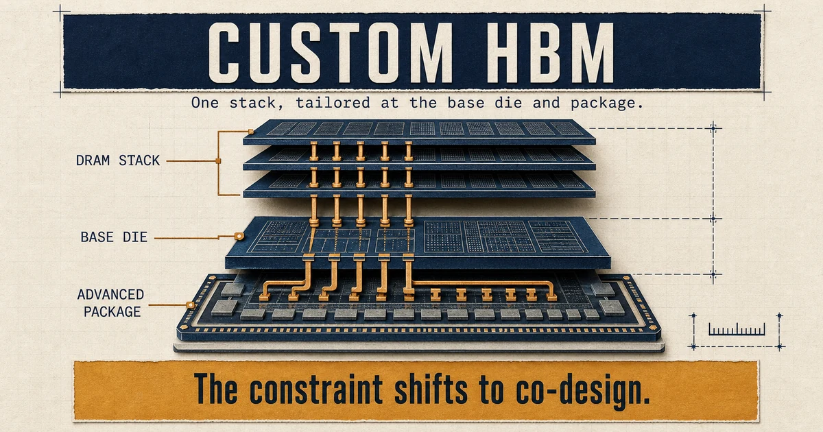
Custom HBM arrives framed as a supply answer, but the harder constraint it creates is a design one, concentrated in the base die at the bottom of each memory stack.
What SK hynix Put on the Roadmap
On July 8, 2026, SK hynix described an HBM roadmap that extends to HBM4E and to what it calls custom HBM. The company’s framing is specific about where customization lives: the base die and packaging are optimized for a given chip architecture, workload, power requirement, and thermal design. In the same material, SK hynix positions HBM not as a standalone part but as one layer inside a wider memory hierarchy.
A separate SK hynix Tech Note explains the mechanism. Different workloads may require differentiated HBM profiles, and a configurable base die can provide those profiles without redesigning the entire stack for every customer. The same note supplies the limiting condition: manufacturing efficiency and yield optimization restrict how many variants can be supported. The vendor’s proposition is therefore bounded customization, not unlimited bespoke silicon.
Portfolio scope completes the picture. At HPE Discover in June 2026, SK hynix presented a lineup spanning HBM, server DRAM, enterprise SSD, and CXL memory. At the TSMC Technology Symposium, it emphasized memory-logic integration, advanced logic processes, custom HBM, and packaging technologies for AI systems. Taken together, these company materials describe HBM as one tier, the base die as a growing configuration surface, and customer co-design as part of the product strategy.
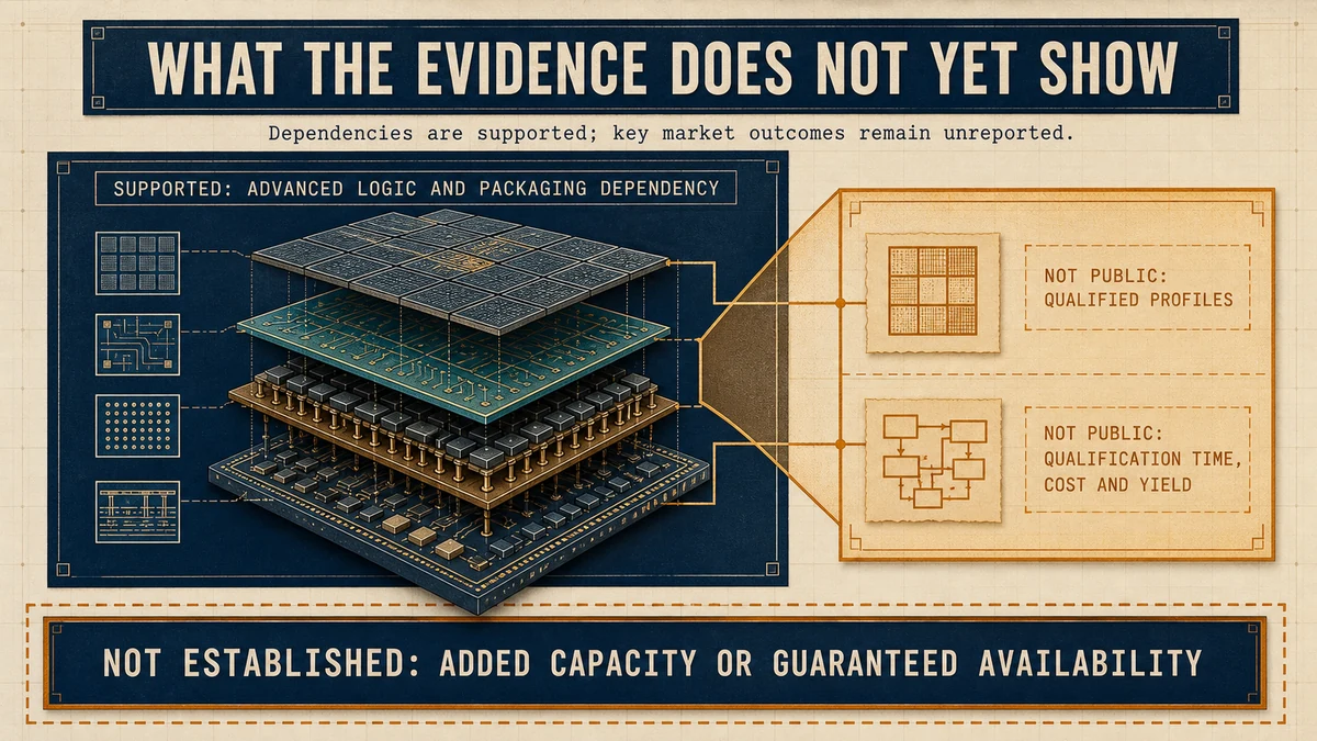
Those statements establish direction, not commercial results. They do not disclose customer adoption, qualification time, pricing, allocation, production volume, or the number of configurations that will reach market. The moving-bottleneck thesis is an interpretation of the mechanism the company describes.
Why Customization Settles in the Base Die
An HBM product stacks DRAM dies above a base die and connects the stack to an accelerator through an advanced package. The base die forms the logic boundary between the memory stack and external processing logic. SK hynix says this layer becomes particularly important with HBM4, where base-die performance can improve connectivity and reduce power consumption.
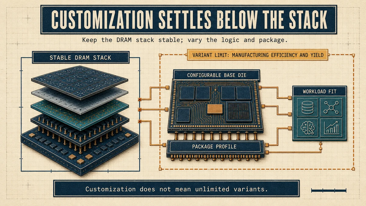
Custom HBM attempts to remove a specific problem: the need to redesign too much of the product whenever a workload needs a different memory profile. Concentrating variation in the base die and packaging allows the expensive, yield-sensitive DRAM stack to remain more consistent. The same basic stack can then be fitted more closely to an accelerator’s architecture, workload, power budget, and thermal envelope.
That is an improvement in fit, not an increase in supply. None of the supplied sources says custom HBM adds wafer capacity, lowers unit cost, guarantees availability, or removes advanced-packaging limits. It changes the layer where engineering variation is introduced. The problem partly removed is repeated full-stack redesign; the problem created is managing more logic and package configurations without losing manufacturing efficiency.
This distinction matters because it changes the buyer’s question. Generic HBM can be compared mainly through capacity, bandwidth, power, and delivery. Custom HBM requires the buyer to ask whether a particular base-die and package profile can be designed, manufactured, validated, and qualified in time for the accelerator program that needs it.
The New Bottleneck Is a Qualified Design Slot
The constraint slides from a common component toward a coordinated design process. Each differentiated base-die profile must pass through architecture definition, logic design, package integration, validation, and qualification. The scarce resource is no longer only DRAM wafers or finished stacks. It can also be the engineering capacity and schedule room required to produce a qualified configuration.
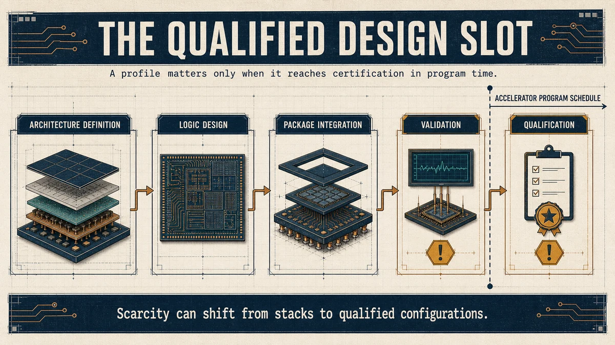
The Tech Note’s warning about manufacturing efficiency and yield gives this bottleneck a physical basis. More variants can divide production learning across more configurations, expand the validation matrix, and make it harder to optimize yield consistently. The sources provide no numerical cost or yield penalty, so that effect should not be quantified. But they do support the narrower conclusion that variant proliferation is constrained by manufacturing economics.
The equipment and materials effect is less specific. SK hynix says it is applying advanced logic process technology to HBM4 base dies through collaboration with TSMC, and its symposium material places HBM beside advanced logic and packaging technologies. That makes logic-process access, assembly, interconnection, and thermal integration part of the custom-HBM dependency chain. No supplied source identifies a particular production tool or material as the bottleneck, so naming one would go beyond the evidence.
Qualification is where those dependencies converge. A memory vendor can offer many theoretical profiles, but a buyer receives value only from one that is stable, manufacturable, and certified for the target accelerator. The meaningful unit of scarcity becomes the qualified design slot: a configuration that can occupy engineering resources, pass validation, and arrive inside a fixed chip-program schedule.
A supplier that can complete that cycle quickly has a stronger claim on the design win. A supplier that offers a wide but unqualified menu does not. Scarcity has not disappeared; it has changed units, from gigabytes and stacks to coordinated design and qualification capacity.
Who Owns the Value and the Risk
Memory suppliers own the clearest commercial opportunity. Co-design gives them earlier access to accelerator roadmaps and makes the relationship harder to replace through a simple spec-sheet comparison. SK hynix’s full-stack framing also suggests a broader account strategy: an HBM relationship could create openings for server DRAM, enterprise SSD, and CXL memory. That portfolio effect is a plausible interpretation, not a disclosed sales result.
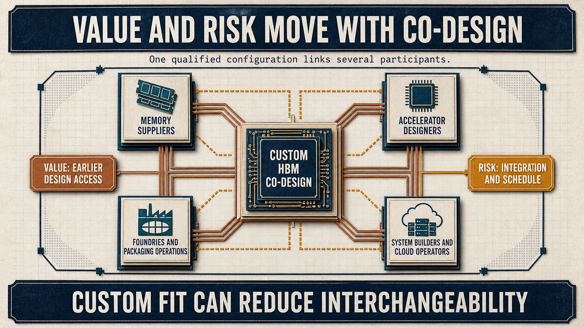
Accelerator designers own the architectural upside and a large share of the schedule risk. Hyperscalers building custom silicon and merchant GPU vendors can pursue a memory profile better fitted to workload, power, and thermal requirements. In return, they must expose those requirements earlier, coordinate decisions with the memory supplier, and absorb the consequences if the joint configuration misses qualification.
Supporting several suppliers also becomes more expensive. Each alternative may require another base-die integration, package path, validation matrix, and qualification cycle. That can increase switching costs even when buyers want supply diversity. A custom configuration fitted to one accelerator generation may also be less fungible across a wider fleet.
Foundries and advanced-packaging operations gain leverage because base-die customization is logic work and the finished HBM must be integrated beside the accelerator. They also inherit execution risk. Access to a suitable logic process is not enough if package integration, power delivery, thermal behavior, or validation delays the finished configuration.
Data-center system builders and cloud operators experience the result as procurement friction. Deeper coupling with a memory supplier can improve architectural fit, but it can also reduce interchangeability and make capacity planning more specific to an accelerator generation. The economic value belongs to the participants that shorten the joint design cycle; the risk belongs to every participant whose schedule depends on that cycle closing successfully.
Qualification Signals and Counterpoints
The next decisive number is not another bandwidth figure. It is how many qualified base-die profiles a supplier can support in one generation, and how quickly each profile can move from architectural requirements to a certified product. The sources do not provide that number, but they identify the conditions that make it worth watching.
- Variant count per generation. A small menu of qualified profiles would support the view that yield and manufacturing efficiency bound customization. A broad catalog delivered without visible friction would weaken it.
- Qualification cadence. Track the interval from architecture definition to a certified base-die and package configuration. A shorter interval would make co-design speed a durable advantage.
- Yield and cost disclosure. Evidence that variant proliferation affects yield learning, validation expense, or unit economics would clarify the price of customization. No numerical estimate is supported by the present sources.
- Logic and packaging access. Delays in base-die processing or advanced packaging would confirm that custom HBM depends on more than DRAM production. The current evidence supports that dependency but not a named equipment or material shortage.
- Portfolio attach. If custom-HBM design wins pull server DRAM, eSSD, or CXL products into the same accounts, the base die is functioning as the commercial wedge suggested by SK hynix’s full-stack strategy.
There are meaningful counterpoints. Accelerator designs could converge on a few standard profiles, reducing the need for repeated customization. Generic HBM could remain preferable when interchangeability, secondary sourcing, or a shorter qualification path matters more than workload-specific fit. Custom HBM also does not itself add capacity, lower cost, or guarantee allocation.
Finally, the evidence is vendor-centered. It contains no confirmed pricing, share, customer count, allocation, qualification duration, or production-volume data. The claim that the bottleneck moves to base-die co-design is this article’s interpretation. SK hynix describes the optimization surface and the wider memory strategy; it does not report that qualified design slots have already replaced capacity as the market’s dominant constraint.
Later in this series
This article is for informational and educational purposes only and does not constitute investment, financial, or legal advice.
Sources
- news.skhynix.com – SK hynix’s HBM4, HBM4E, custom-HBM, base-die, packaging, and full-stack memory direction. (2026-07-08)
- news.skhynix.com – Workload-specific profiles, configurable base-die logic, and manufacturing-efficiency and yield limits on variant proliferation. (2026)
- news.skhynix.com – Portfolio spanning HBM, server DRAM, enterprise SSD, and CXL memory. (2026-06)
- news.skhynix.com – SK hynix’s presentation of memory-logic integration, custom HBM, advanced logic processes, and advanced packaging. (2026-04-23)