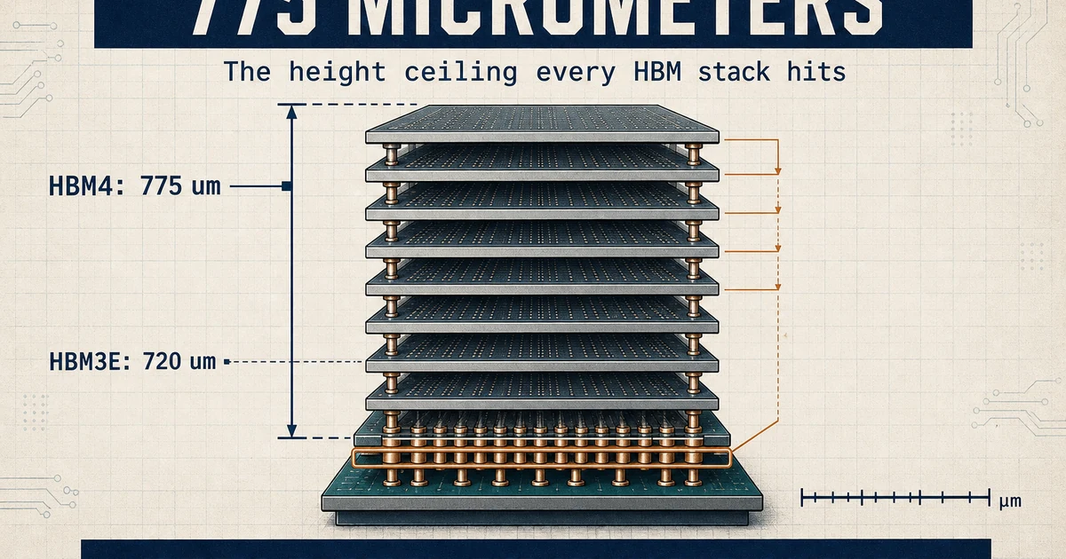
775 micrometers. That is the total height a high-bandwidth memory stack is allowed to reach – the thickness of a standard 300mm logic wafer, and the ceiling every HBM generation has been pushing against since JEDEC last widened it, from 720 micrometers, to make room for HBM4. Every DRAM layer added above the current count has to come from a die that is thinner, and a gap between dies that is narrower, than the layer below it.
Picture packing more sheets of paper into a binder whose spine cannot get any wider: at some point you stop being able to add paper and start having to swap in a thinner grade instead. Memory makers are at that point now. There is one known way past it – hybrid bonding, which fuses copper pads directly between dies with no solder bump and no underfill gap to fill – and two of the world's memory suppliers just told a room full of engineers, in the same week, two different things about how close it actually is.
The Wall Every HBM Generation Hits First
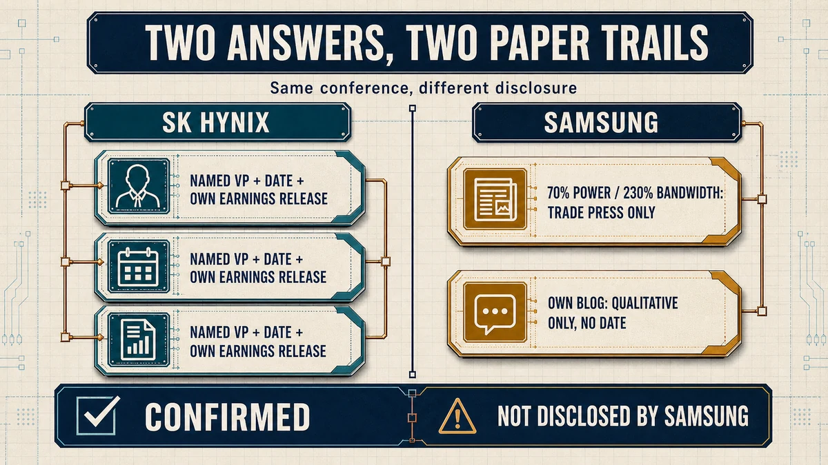
At Hot Chips 2026 on August 23, SK hynix's VP of package engineering, Jaesik Lee, said the company does not expect hybrid bonding to be ready for HBM4E, the generation shipping next – pushing the industry's most anticipated packaging transition out to HBM5 at the earliest. The reason he gave was not cost and not customer demand. It was the bond itself: producing reliable copper-to-copper joints across 16 or 20 stacked memory dies, at that 775-micrometer height budget, remains an unresolved manufacturing problem.
SK hynix's current process – Mass Reflow Molded Underfill, or MR-MUF – will instead carry the company's 16-high HBM4 (already in customer qualification) and its HBM4E generation, extended all the way through Nvidia's next GPU platform.
What July Expected and What August Confirmed
That date did not fall out of nowhere. Five weeks earlier, this desk argued from the JEDEC spec change alone that the industry was not equipment-ready for a harder version of this same bond – Samsung's zHBM concept, which asks for memory bonded directly onto a live logic die. What was missing then was a company willing to put its own name and date on the delay.
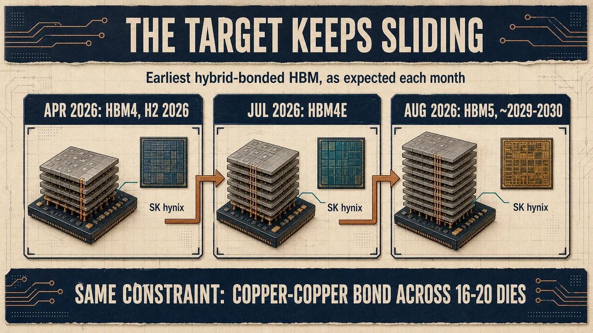
Hot Chips supplied it, and the run-up shows the target sliding later all year. In April, SK hynix had just finished validating 12-high hybrid-bonding HBM at the pilot stage – no disclosed yield numbers, but a technical lead calling the company "significantly better prepared than it was two years ago" – while the wider industry still expected a gradual hybrid-bonding introduction starting with HBM4 in the second half of 2026. By July, that expectation had already retreated one generation, to 16-high HBM4E as the earliest realistic adoption point.
By August, SK hynix's own conference statement retreated it a full generation further, past HBM4E entirely, to HBM5. A prediction that keeps moving later on the same axis, made by the company that would have to build it, is not noise – it is the clearest evidence available that the bond is the actual constraint, not the memory cell or the interposer around it.
The Business Already Riding on the Conservative Bet
This is not a hedge SK hynix is making with idle capacity. The company holds an estimated 70% of Nvidia's HBM orders for the Vera Rubin generation, and all of it is planned to ship on MR-MUF. SK hynix's own 2Q26 earnings release, published three and a half weeks before Hot Chips, said HBM4 mass production began that quarter for key customers, with a broader ramp planned for the second half, and that HBM4E has "demonstrated its differentiated technological edge" in samples already shipped.
On the same earnings call, the company said HBM4's mass-production yield and quality were "showing levels close to HBM3E, which has already entered a mature stage" – a maturity claim, not a disclosed percentage, but a real one: it is describing a process already earning revenue, not a lab result.
SK hynix is not standing still on the harder bond, either. In March, before any of this, it placed its first mass-production-grade hybrid-bonding equipment order – a roughly 20-billion-won ($14-15 million) inline system combining Applied Materials' polishing and plasma tools with a Besi hybrid die bonder, the same tool pairing already running in volume at TSMC to build AMD's 3D V-Cache. An industry official close to the order called it preparation for "the next-next generation," not the current one.
That is the shape of a company buying the equipment years before it plans to need it commercially – confident about the direction, unwilling to bet the current product cycle on the timing.
Samsung's Numbers, and Where They Haven't Appeared Yet
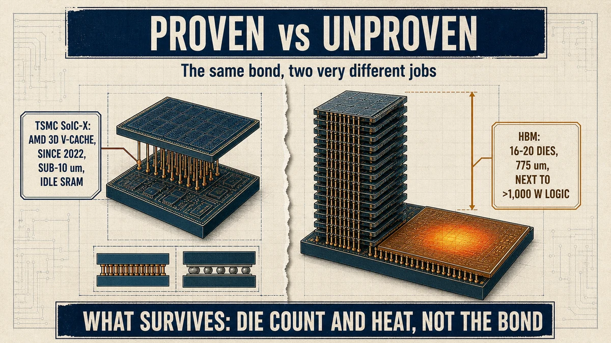
Samsung took the opposite side of the same conference. Its zHBM concept goes further than the DRAM-to-DRAM hybrid bond SK hynix just deferred – it proposes stacking the memory directly onto the compute die itself, eliminating the interposer between them entirely, in a wafer bond that has to survive next to well over 1,000 watts of logic heat rather than sit beside it.
Trade press covering Samsung's Hot Chips technical session reported specific numbers: 70% higher power efficiency and 230% greater DRAM bandwidth than a standard HBM4e stack, with one cited example showing four zHBM stacks paired with a 1,200-watt GPU saving roughly 100 watts.
Here is the detail the headline numbers skip past. Samsung's own official channel – a company tech-blog post about zHBM from its FMS 2026 keynote, published nine days before Hot Chips – describes the same architecture only in qualitative terms: it "integrates logic and memory in 3D to reduce the physical distance data must travel," with no power-efficiency percentage, no bandwidth multiplier, and no production timeline attached. The 70% and 230% figures exist, independently reported by more than one outlet covering the same technical session. They do not yet exist in anything Samsung itself has published.
Data
| Company | Claim | Disclosed by | Timeline stated | Status |
|---|---|---|---|---|
| SK hynix | Hybrid bonding not ready for HBM4E; earliest is HBM5 | Named VP, Hot Chips 2026 | 2029-2030 (industry forecast) | confirmed |
| SK hynix | HBM4 mass-production yield/quality near HBM3E maturity | Company earnings call | Current (2Q26) | confirmed (qualitative; no % disclosed) |
| Samsung | zHBM: 70% power efficiency, 230% bandwidth vs. HBM4e | Trade press, Hot Chips session | Not stated | not disclosed by Samsung itself |
| Samsung | zHBM architecture and rationale | Samsung's own tech blog, FMS 2026 | Not stated | confirmed (qualitative only) |
The Gap That Would Actually Prove Someone Right
The honest counter to all of this is that hybrid bonding is not experimental technology in general. TSMC has been hybrid-bonding AMD's 3D V-Cache in high volume since the Ryzen 7 5800X3D shipped in 2022, at sub-10-micron pitch, with no solder bump in the joint at all. A company with Samsung's process resources could plausibly have real internal validation behind its zHBM numbers and simply not have chosen to publish it through an investor-facing channel yet – corporate disclosure timing is not the same thing as technical readiness.
But that counter cuts in a specific, checkable direction: it says the gap is a disclosure gap, not a physics gap, and disclosure gaps close on their own schedule if the numbers are real. Samsung publishing its own 70% and 230% figures through an official newsroom or investor release, with a production date attached, would close it. So would a named accelerator customer announcing an actual hybrid-bonded HBM qualification ahead of SK hynix's stated window, or a second hybrid-bonding equipment supplier shipping production-grade tools faster than Besi and Applied Materials currently are. None of those has happened yet.
What has happened is that the company selling into next year's GPU platform chose the process it already knows how to run, and said so on the record with a name and a date attached – and the company with the more dramatic numbers has, so far, only said so through someone else's coverage of a conference room.
Bottom Line
The bonding technology at the center of this is proven – TSMC has shipped it in volume for three years. What is not yet proven is which of two Korean suppliers' HBM roadmap claims describes what actually ships next, and right now only one of them has attached its name to a date. Nvidia's current generation is already built on the answer SK hynix gave. Whether Samsung's answer arrives with the same kind of paper behind it is the thing worth checking the next time either company reports.
Sources
- tomshardware.com — SK hynix's Hot Chips 2026 statement delaying hybrid bonding to HBM5, the 775-micron ceiling, MR-MUF extension through Nvidia Rubin, ~70% of Rubin HBM orders (2026-08-23)
- trendforce.com — Samsung's zHBM power-efficiency/bandwidth figures and architecture description from Hot Chips 2026 (2026-08-24)
- trendforce.com — July industry forecast naming 16-high HBM4E as earliest hybrid-bonding adoption point; JEDEC 720-to-775-micron spec change (2026-07-07)
- news.skhynix.com — SK hynix's own 2Q26 earnings release: HBM4 mass production start, HBM4E sample status (2026-07-29)
View all sources
- en.sedaily.com — SK hynix earnings-call statement on HBM4 yield/quality nearing HBM3E maturity (2026-07-29)
- en.sedaily.com — Industry forecast (Counterpoint Research) of SK hynix HBM5 launch and hybrid-bonding mass production around 2029-2030 (2026-04-06)
- semiconductor.samsung.com — Samsung's own official zHBM description from its FMS 2026 keynote, qualitative only (2026-08-14)
- thelec.net — SK hynix's first mass-production-grade hybrid-bonding equipment order (Applied Materials/Besi) (2026-03-31)
- trendforce.com — SK hynix's 12-high hybrid-bonding HBM validation status and industry adoption expectations as of April 2026 (2026-04-29)
- semianalysis.com — TSMC SoIC-X hybrid bonding in mass production for AMD's 3D V-Cache since 2022 (counterargument precedent) (2024-02-09)
This article is for informational and educational purposes only and does not constitute investment, financial, or legal advice.