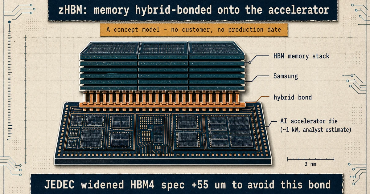
Samsung zHBM would hybrid-bond a memory stack directly onto the AI accelerator itself – the same year JEDEC quietly widened HBM4's spec by 55 micrometers specifically to avoid doing that inside a memory stack at all.
The Spec That Bought a Generation More Time
JEDEC, the industry body that sets HBM's physical dimensions, raised the maximum module height from 720 micrometers for HBM3E to 775 micrometers for HBM4, with a further ceiling proposed up to 1,000 micrometers for HBM5. The extra 55 micrometers sounds trivial. It is not. That margin is precisely what let 16-high HBM4 keep using conventional microbump bonding – heating solder balls to fuse dies – instead of moving to hybrid bonding, which fuses copper pads directly without solder.
The reasons, corroborated independently by two separate outlets reading the same underlying decision, are unglamorous and specific: hybrid bonding requires "the reconstruction of new equipment, materials, and testing processes," raising per-package cost; SK hynix's own internal evaluation reportedly found that "given the current yield pressure and cost balance, the inertia of mature processes is still strong"; and a fluxless bonding transition technology "encountered more difficult real-world problems than expected in the mass-production stage". Demand for 16-high stacks also arrived slower than customers like Nvidia had signaled, easing the pressure to force the transition.
Samsung and SK hynix each built stopgap thermal fixes – a Heat Path Block and an ICE-based design, respectively – rather than bond their way past the heat problem. Hybrid bonding is now expected no earlier than 16-high HBM4E, and industry reporting suggests it could slip further.
That is the industry's own answer, arrived at collectively through a standards committee, to whether hybrid bonding was ready for the easy case: DRAM die bonded to DRAM die, inside one memory stack, with both sides made of the same material and running at comparable, modest power.
What zHBM Actually Proposes
Samsung's answer to a related but distinct problem – how to feed an AI accelerator's growing appetite for bandwidth – goes further, not more cautiously. At FMS 2026 in Santa Clara, Samsung's own newsroom described zHBM and zNAND-O as "the industry's first concept models," with zHBM stacking HBM vertically "directly above AI accelerators, rather than positioning it alongside processors," using what the company calls next-generation wafer bonding. The claimed numbers are large: roughly 8x the performance of HBM5, more than 10 times the memory density, threefold energy efficiency, and thermal resistance cut by more than half.
Those figures are not new to August. Samsung first showed the same architecture in February 2026 at SEMICON Korea, where it claimed "more than 4x higher bandwidth and 75% lower power consumption". By the August reveal, with no production milestone in between, the framing had grown to roughly double the bandwidth multiplier. That pattern – a concept getting a bigger number before it gets a customer – is worth noting on its own, independent of whether either figure eventually holds.
It is also worth separating what actually shipped from what did not. The same FMS announcement bundled zHBM and zNAND-O with V10 BV-NAND, a 400-plus-layer NAND design already in mass production and, according to a July 2026 report, already supplying Nvidia. V10 is a real, shipping product. zHBM and zNAND-O are not; Samsung's own materials name no customer and no production date.
The engineering reason to want zHBM at all is a real physical constraint some analysts describe with a specific shorthand: "beachfront." Every HBM stack in production today reaches the GPU across an interposer, through space at the edge of the die – and that edge space is running out, because it grows only as fast as the die's perimeter while the accelerator's appetite for bandwidth grows with its full compute area. Removing the interposer and bonding memory straight onto the logic die is, in principle, one way past that ceiling.
A Harder Version of the Bond the Industry Just Avoided
In principle is doing a lot of work in that sentence. An independent analysis lays out three specific gates zHBM would have to clear before it could ship: extracting roughly a kilowatt of heat through a stacked DRAM die without degrading it – called the tallest of the three hurdles; scaling the bonding pitch below 10 microns at production yield; and completing known-good-die testing before an irreversible bond, since a defect discovered after bonding cannot be reworked the way a socketed or interposer-mounted component sometimes can.
The same analysis flags Samsung's headline thermal figure specifically: "a vendor-supplied figure" that "is the number that most needs independent validation". It is the same conclusion this desk reached about a different packaging layer – a supplier's yield number carries no information until its measurement boundary is stated – applied here to a thermal claim instead of a yield claim.
Set those three gates against what JEDEC just did for the easier version of the same underlying technology, and the contrast sharpens. If the industry's own standards committee – whose membership includes Samsung – judged hybrid bonding too costly and yield-constrained to force into DRAM-to-DRAM bonding this generation, a chip-on-logic bond carrying an order of magnitude more heat and permanently joining memory to the single most expensive die in the package is a considerably harder claim to make on a concept model.
Samsung's own memory rival made a visibly more conservative choice on the identical problem. SK hynix's iHBM, unveiled in May 2026, embeds a silicon-based cooling element inside the existing HBM package to cut thermal resistance by 30 percent – a smaller number than Samsung's claimed 50-plus percent – but does so using what the company calls "market-proven Mass Reflow Molded Underfill technology," fitting inside its already-qualified manufacturing process rather than adopting a new bonding technology.
One Korean memory maker chose the larger, unproven number; the other chose the smaller, provable one, inside a process it already knows how to run at yield. That divergence, more than either company's press release, is the clearest signal of how differently the industry is pricing this risk. It is also a continuation of a bottleneck this desk has tracked moving deeper into the package with each generation: custom HBM's base-die layer already shifted the constraint to co-design and qualification; zHBM would shift it again, onto the bond joining memory to the compute die itself.
Who Builds the Bond
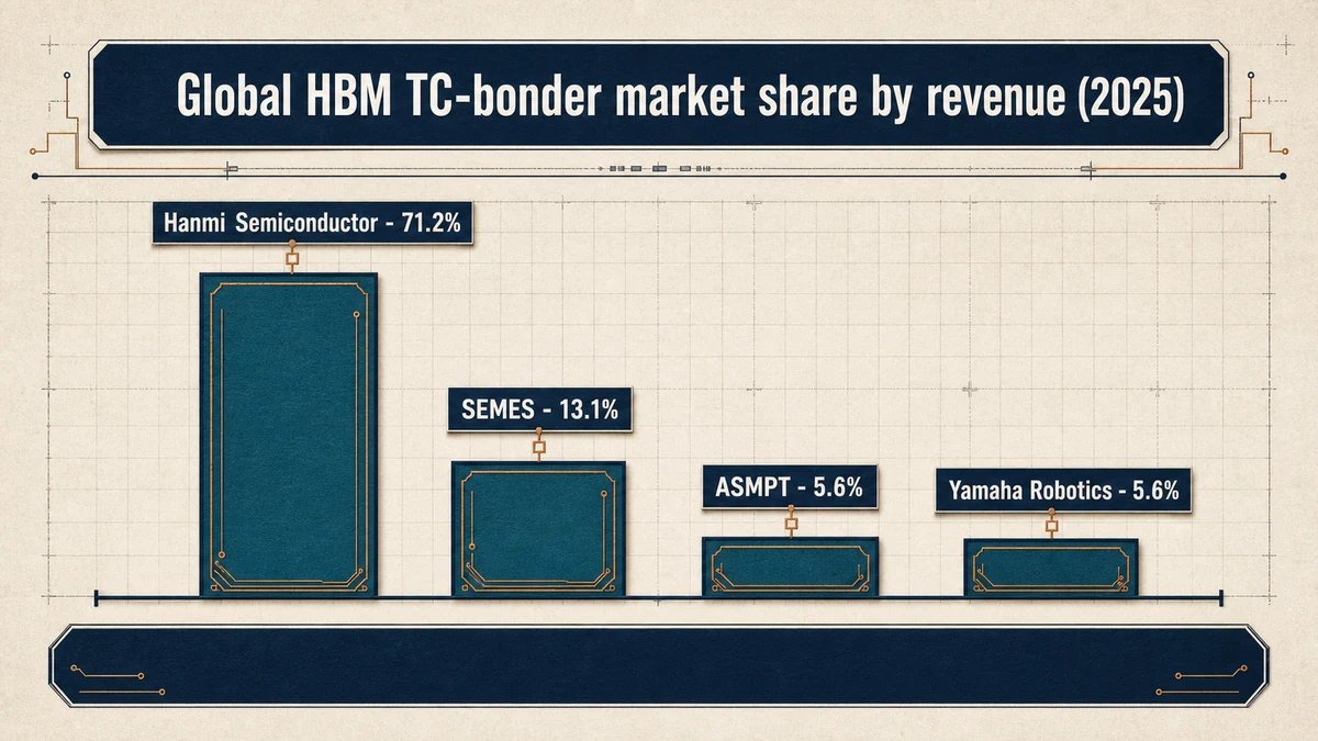
A concept model needs more than a validated thermal number to become a shipping part – it needs equipment that can actually perform the bond, at volume, at yield. Hanmi Semiconductor is the dominant supplier of the thermo-compression bonders used across HBM production today, holding a 71.2 percent global revenue share according to TechInsights' 2025 TC Bonder Market Report, well ahead of SEMES (13.1 percent), ASMPT (5.6 percent) and Yamaha Robotics (5.6 percent).
| Supplier | HBM TC-bonder revenue share |
|---|---|
| Hanmi Semiconductor | 71.2% |
| SEMES | 13.1% |
| ASMPT | 5.6% |
| Yamaha Robotics | 5.6% |
That concentration matters because Hanmi's own hybrid-bonding line is not yet running. The company plans to launch a second-generation hybrid bonder prototype for next-generation HBM "within the year," with dedicated hybrid bonder factory operations not beginning until the first half of 2027. If zHBM or anything like it is going to be built at volume, it most likely runs, at least initially, through equipment that has not finished being built. That is a calendar fact, not a simulation result, and it sits underneath every performance multiple Samsung has published so far.
The ripple from that equipment gap reaches well past memory makers.
Foundries and OSATs that assemble AI accelerators would need to requalify their packaging lines around a fundamentally different bonding step; data-center cooling vendors already redesigning around liquid and immersion cooling for standard HBM stacks would face an even denser, more concentrated heat source directly on the compute die; and GPU and custom-silicon teams at Nvidia, AMD and the hyperscalers would need to co-design their next accelerator generation around a memory architecture that cannot be reworked once bonded, raising the cost of a packaging mistake on the most expensive part of the system.
The Precedent That Cuts Both Ways
The strongest case against treating zHBM as vaporware is that chip-on-chip hybrid bonding is not unproven technology in general. TSMC's SoIC process has fused AMD's 3D V-Cache SRAM die onto its compute chiplet in high-volume production since the Ryzen 7 5800X3D launched in April 2022, at sub-10-micron bond pitch. Four-plus years of shipping volume is a real, checkable track record, and it is the fair rebuttal to any suggestion that hybrid bonding itself is science fiction.
What that precedent does not establish is that the same joint survives zHBM's specific demands. AMD's stacked cache die is thin, draws relatively little power beyond leakage, and sits on a CPU chiplet running well under 150 watts. zHBM proposes bonding a taller, multi-die, actively heating HBM stack onto an accelerator that one analysis places at roughly a kilowatt – a difference in thermal load closer to an order of magnitude than a scaling step, on a bond that, once made, cannot be reopened.
TSMC's own packaging platform reflects that gap in confidence: its CoWoS interposer service, not a chip-on-logic alternative, is still what the foundry is expanding, with certification of larger 5.5x-reticle interposers completed in 2025 and volume production planned for 2026. The company building most of the world's AI accelerators has not repositioned the interposer as a technology on its way out – the pattern this desk has also traced in how advanced packaging keeps redistributing risk across partitioning, testing and thermal design rather than collapsing it into one solved layer.
None of this means zHBM is a dead idea. It means the claim that would settle the question – a validated thermal number measured under sustained training load, not simulation, alongside bonding equipment actually running at volume – does not exist yet, and the two clearest paths to it (Hanmi's factory, or a customer qualification program) both point toward 2027 at the earliest. Until one of those arrives, the bond a reader should watch is not the one Samsung demonstrated on a show floor. It is the plainer one JEDEC just chose not to make.
Sources
- news.samsung.com — Samsung's own zHBM/zNAND-O/V10 BV-NAND claims, concept-model status, mechanism description (2026-08-05)
- trendforce.com — February 2026 preview figures vs. August 2026 reveal figures for zHBM (2026-08-05)
- futurumgroup.com — "Beachfront" mechanism, three production gates, thermal-figure skepticism (2026-08-05)
- note.com — JEDEC HBM module-height spec relaxation, reasons and revised hybrid-bonding timeline (2026)
View all sources
- eu.36kr.com — Independent corroboration of JEDEC spec numbers; cost/yield reasoning, SK hynix evaluation quote (2026)
- prnewswire.com — SK hynix iHBM official technical details and manufacturing basis (2026-05-26)
- semiconductor-digest.com — Hanmi Semiconductor hybrid bonder prototype and factory timeline (2026)
- asiae.co.kr — Hanmi Semiconductor TC bonder market share and competitor shares (2025-12-22)
- amd.com — AMD Ryzen 7 5800X3D / TSMC SoIC hybrid-bonding production precedent (2022-03-15)
- tsmc.com — TSMC's continued CoWoS interposer investment and roadmap (2026 (evergreen page))
- trendforce.com — V10 BV-NAND mass-production status, contrast with zHBM/zNAND-O concept status (2026-08-05)
🇰🇷 Read this analysis in Korean (한국어판 보기)
This article is for informational and educational purposes only and does not constitute investment, financial, or legal advice.